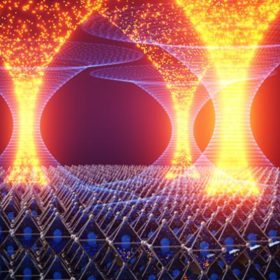
Tuning out the defects for more powerful perovskite solar cells
Scientists in the UK and Japan used the latest imaging techniques to observe the inner workings of a perovskite solar cell at the scale of a few nanometers. Their findings suggest that a single defect is responsible for both limiting initial performance and causing degradation of the cell. By altering chemical compositions and process parameters, the appearance of this defect can be quickly reduced, and the group is confident that its finding could quickly be applied in large-scale processing as well.
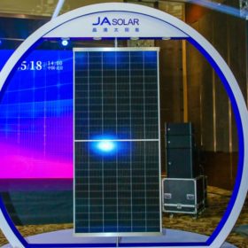
JA Solar introduces n-type solar panel with 22.4% efficiency
JA Solar said that the smallest solar panel in its new n-type product line has a power output of 435 W and a power conversion efficiency of 22.3%. The largest module in the series has an efficiency rating of 22.4% and 625 W of nominal power. Their temperature coefficient is -0.30% per degree Celsius.
Canadian Solar plans to ramp up production capacity
Having warned of in-house solar wafer and cell capacity as recently as the third quarter of 2021, the company has announced it will be adding even more production lines this year.
Chinese PV Industry Brief: Geely opens polysilicon plant
Automaker Geely has commissioned a new polysilicon factory in northern China, while ET Solar has opened a new 5 GW wafer factory in Vietnam. Poly giant GCL Technology, meanwhile, has confirmed that its board might issue common stock for a Chinese listing.
JinkoSolar showcases 13.08%-efficient transparent TOPCon solar module for BIPV, agrivoltaics
The new solar module can be purchased with different levels of transparency, depending on the project, with light transmittance ranging between 30% and 40%. It has a power output of 245 W to 300 W and a temperature coefficient of -0.30% per C.
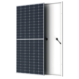
Hanersun launches 580 W TOPCon solar module with 22.38% efficiency
Hanersun claims that its new TOPCon solar modules are suitable for residential and commercial rooftops, as well as small-scale, ground-mounted PV plants. They have a temperature coefficient of 0.31%.

Kiwa Deutschland acquires PI Berlin
Kiwa Deutschland has acquired PI Berlin for an undisclosed sum, but the technical consultancy will retain its name and structure.

‘Extraordinary week’ capped off with PV-IPCEI launch in Brussels
The PV-IPCEI event hosted by the European Solar Manufacturing Council (ESMC) took place on May 20 in a narrow wood-paneled room of Brussels’ Art Deco Residence Palace.
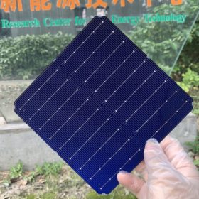
Heterojunction solar cell with 25.18% efficiency, 85.42% fill factor
Researchers in China have fabricated a heterojunction solar cell with a 244.63 cm2 Czochralski n-c-Si wafer. They used light soaking to improve the dark conductance of the hydrogenated amorphous silicon films.
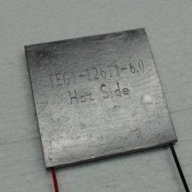
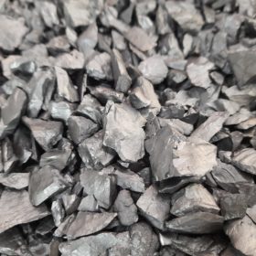
Upcycling silicon waste from end-of-life solar panels into thermoelectrics
Researchers in Singapore have developed a new technique in which polycrystalline silicon is pulverized into powder and pelletized into ingots. The process relies on spark plasma sintering to dope the silicon with germanium and phosphorus.
