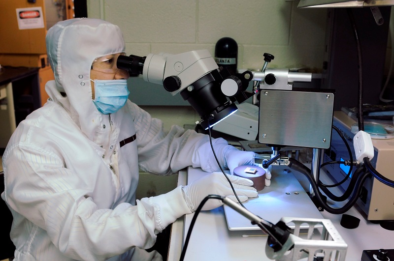
Silicon solar cells have enjoyed incremental efficiency increases over the past few years, with many now able to convert up to 25% of sunlight into electricity. However, manufacturing silicon wafers, which need to be around 300 microns thick to absorb all the sunlight that reaches them, requires temperatures of around 1,200 degrees Celsius, a procedure that brings significant costs. Telluride, a cheaper alternative to silicon, is however highly toxic and known to cause cancer.
Such conditions prompted Goutam Dalapati and other colleagues from Singapore’s A*STAR institute of Materials Research & Engineering to investigate a copper-zinc-tin-sulfide (CZTS) compound, which offers the optical and electrical properties required in solar cells, and is made from non-toxic, widely available materials that are cheaper than silicon to process.
“CZTS is a semiconducting compound with a higher absorption coefficient than silicon,” says Dalapati, “so it's able to absorb more visible light and produce more electricity than silicon, and can be used for very large-scale applications, like roofs and solar farms.”
Solar cells made from CZTS have the potential for up to 30% efficiency, he claims. However, they require high-quality, thin film of CZTS with no impurities, and a suitable material for the interface layer that sits underneath the CZTS, helping to collect electrical charge.
Popular content
The thin films of CZTS were grown using a technique called quaternary sputtering, where a single target made from CZTS was used as a source for depositing the film.
There are several advantages offered by this method over deposition methods. These include excellent uniformity over large areas and reduced reliance on toxic precursors.
“The composition and structural properties of the CZTS layer depend on the deposition process and the sulfurization,” explains Dalapati. “By using a single-step sputtering target we were able to produce a thin film with a uniform composition and smooth surface, which limits the formation of defects, and is a highly reproducible process.”
This content is protected by copyright and may not be reused. If you want to cooperate with us and would like to reuse some of our content, please contact: editors@pv-magazine.com.


1 comment
By submitting this form you agree to pv magazine using your data for the purposes of publishing your comment.
Your personal data will only be disclosed or otherwise transmitted to third parties for the purposes of spam filtering or if this is necessary for technical maintenance of the website. Any other transfer to third parties will not take place unless this is justified on the basis of applicable data protection regulations or if pv magazine is legally obliged to do so.
You may revoke this consent at any time with effect for the future, in which case your personal data will be deleted immediately. Otherwise, your data will be deleted if pv magazine has processed your request or the purpose of data storage is fulfilled.
Further information on data privacy can be found in our Data Protection Policy.