A research group from Japan’s Tokyo Institute of Technology and Waseda University has developed a new technology for the production of thin film monocrystalline solar cells, which is expected to significantly reduce the costs of mass production, while maintaining high levels of cell efficiency.
The scientists claim they were able to develop what they call a high-quality thin film monocrystalline silicon, which has a thickness of approximately 10 μm and a reduced crystal defect density.
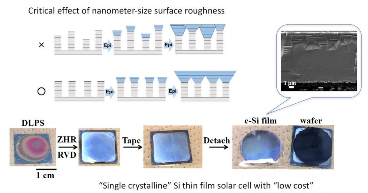
The silicon density, they further claim, was reduced to the silicon wafer level at a growth rate that is more than 10 times higher than previously achieved.
This result, the research team explains, was obtained by smoothing the surface to a roughness of 0.2 to 0.3 nm through a zone heating recrystallization method (ZHR method). The resulting substrate was then used for high-speed growth to create a monocrystalline thin film with high crystal quality.
“The grown film can easily be peeled off using the double-layer porous Si layer, and the substrate can be reused or used as an evaporation source for thin film growth, which greatly reduces material loss,” the researchers added.
This process also showed, according to the scientists, that a surface roughness in the range of only 0.1-0.2 nm has an important impact on the formation of crystal defects, which is also of interest as a crystal growth mechanism.
“The use of this Si thin films as low cost bottom cells in tandem type solar cells with an efficiency of over 30% will also be considered,” the Japanese scientists asserted in their statement.
This content is protected by copyright and may not be reused. If you want to cooperate with us and would like to reuse some of our content, please contact: editors@pv-magazine.com.


By submitting this form you agree to pv magazine using your data for the purposes of publishing your comment.
Your personal data will only be disclosed or otherwise transmitted to third parties for the purposes of spam filtering or if this is necessary for technical maintenance of the website. Any other transfer to third parties will not take place unless this is justified on the basis of applicable data protection regulations or if pv magazine is legally obliged to do so.
You may revoke this consent at any time with effect for the future, in which case your personal data will be deleted immediately. Otherwise, your data will be deleted if pv magazine has processed your request or the purpose of data storage is fulfilled.
Further information on data privacy can be found in our Data Protection Policy.