Heterojunction (HJT) cell technology combines the advantages of monocrystalline silicon (c-Si) solar cells with the good absorption and superior passivation characteristics of amorphous silicon (a-Si), which have been observed in a-Si thin film technology using readily available materials. The HJT design is not new. Sanyo (now Panasonic) first pushed this technology into mass production more than 20 years ago, achieving around 20% cell efficiency.
Recently Panasonic demonstrated efficiencies of 24.7% on laboratory-scale cells. With the discontinuation of the basic technology patent, heterojunction technology was opened to the public in 2010. Meyer Burger is now offering this appealing technology as a high performance key technology in the photovoltaic value chain and promises an average intrinsic cell efficiency of 23-24% in mass production.
The thin intrinsic hydrogenated amorphous silicon (a-Si:H) layers deposited between c-Si wafer and doped layers are key to achieving maximum performance from the cell structure. These achieve reduced interface state density, decreased surface recombination losses, and lower emitter saturation currents.
HJT cell production is a relatively straightforward process, which takes place at low temperatures and requires fewer production steps compared to many other high efficiency designs – including PERC, metal wrap through, and selective emitter. This makes HJT economically attractive, as it can result in significant energy cost savings.
An important technological advantage of HJT cells is the excellent surface passivation of a-Si:H, which results in high open-circuit voltages and high cell efficiencies. The superior temperature coefficient of TC = -0.25%/K ensures higher energy yield during module operating conditions. Compared to standard c-Si technology, heterojunction cells generate 35% more kWh/m2 and therefore reach the lowest levelized cost of electricity (LCOE).
As previously mentioned, low temperature processing (< 250°C) saves energy during manufacturing, prevents bulk degradation, and enables the use of thin wafers. Integrated development throughout the PV value chain – diamond wire wafering, heterojunction cell technology, and SmartWire Connection Technology (SWCT) – guarantees the maximum performance of HJT modules.

Thin wafers
Today, wafers with a thickness of around 180 micrometers (µm) are in standard use in cell manufacturing. Using thinner wafers leads to significantly lower material costs, because a higher number of wafers can be cut from one brick. With decreasing wafer thickness, the influence of the bulk material quality also decreases, resulting in less tight requirements for, as an example, minority charge carrier lifetimes. The use of diamond wire sawing in wafer production leads to fewer microcracks, and the depth of the microcracks is shallower. With decreasing wafer thickness and the corresponding higher surface to bulk ratio, the surface recombination loss becomes dominant compared to recombination loss in the bulk. Consequently, superior surface passivation techniques are mandatory. Meyer Burger promises an excellent surface passivation with its HELiAPECVD system which enables increasing cell VOC for thin wafers and balancing the loss of ISC due to lower light absorption.
Process flow/Texturing
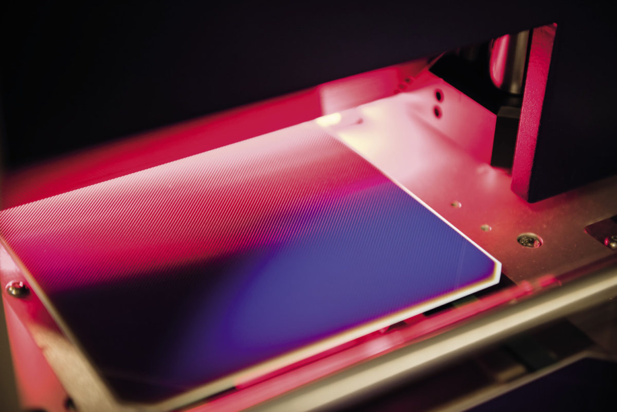
An optimal texturing and cleaning process forms the basis for a successful production process for highly efficient HJT cells. Meyer Burger’s process know-how sets the foundation for optimum passivation. The initial steps in the HJT process sequence are wet chemistry processes for saw damage removal (SDR), texturing, cleaning, and hydrogen termination. The subsurface damages and microcracks have to be almost completely removed to achieve high efficiency HJT cells. Measuring the surface recombination velocity (SRV) indicates the necessary saw damage removal independent of the quality of the bulk. Figure 4 shows the impact of saw damage removal on the surface recombination velocity.
The saw damage removal can be optimized with the texturing process. A final short dip in hydrofluoric acid terminates the silicon surface until final passivation in the subsequent PECVD process. The surface after this wet chemical treatment is crucial for the quality of the c-Si/a-Si:H interfaces and therefore for the surface passivation.
PECVD: a-Si:H coating for the front and rear sides
In order to minimize energy loss within the solar cell, the surface must be highly passivated. Low temperature passivation with a-Si:H deposited in a temperature range between 150 and 250°C results in outstanding surface recombination velocities. This a-Si:H is able to passivate all levels of n-type and p-type silicon. Doped a-Si:H is used to form both the emitter and the back surface field (BSF). Additionally, doped a-Si:H contributes to passivation due to its field effect properties.
Meyer Burger has developed the modular high throughput HELiAPECVD system specifically for wafer-based silicon HJT cell concepts. The heart of the HELiAPECVD system is the patented S-Cube, a sophisticated parallel plate plasma reactor with a box-in-box arrangement providing ultra-pure and uniform amorphous silicon layers. A 13.56 MHz RF source is used to minimize plasma damage during layer deposition. Thus, the required quality of the amorphous silicon layers in terms of minority charge carrier lifetime and band gap is ensured. The key parameter to determine the quality of the passivation with the a-Si:H layer is the minority charge carrier lifetime.
PVD: TCO/metal coating for rear side contact
In the modular HELiAPVD system, a sputter process is used in one of the chambers to apply a transparent conductive oxide (TCO) layer to the front and rear sides of the wafer. In addition to collecting the photo-generated current and forming an ohmic contact on the cell, the TCO layer on the front side acts as an anti-reflection layer. Especially for the front side of the HJT cell, the optical and electronic properties of a-Si:H and TCO layers need to be adjusted with respect to each other.
Indium tin oxide (ITO) is a favorable TCO material for HJT cells because it is very transparent and conductive while providing a good electrical contact with the doped a-Si:H layers. In a second chamber of the same HELiAPVD system, another TCO layer is applied on the back side of the cell with 95% bifaciality. The bifacial cell can also be used in a monofacial solar module where the white back sheet reflects the light back to the cell and increases general module power. This is accomplished without having to break the vacuum or to turn the wafer between these coating processes. The HELiAPVD system configured for HJT cell processing enables edge isolation while simultaneously avoiding extra laser or chemical steps. Rotating cylindrical sputter targets for TCO and metals on magnetrons enables a high target utilization of over 85% to be achieved, ensuring a cost-effective coating process. The HELiAPVD and HELiAPECVD systems are perfectly matched in terms of capacity and layer properties.

Print front side
Conventional crystalline silicon solar cell technologies use front side collector lines (“fingers”) and busbars. Reducing the consumption of the silver paste used in the fingers and busbars is another key step to reducing costs.
Meyer Burger offers the busbarless SmartWire Connection Technology (SWCT) to minimize cell-to-module (CTM) loss and to optimize the module efficiency. Only the finger grid pattern on the front surface of HJT cells will be formed by using a conventional screen printer and an epoxy-based low temperature paste. The busbarless design facilitates a fine-lined screen printed grid pattern. By replacing the busbars with a lined grid pattern with thinner and smaller fingers, silver consumption is significantly reduced. It also increases the cell conversion efficiency by decreasing shadow loss on the cells.
With the application of SWCT, the requirements for finger conductivity become less stringent compared to the requirements for conventional busbar designs. A finger resistance of up to 100 ohms/cm can be combined with SWCT without causing significant power losses. The shorter the distance between two finger contacts, the lower the impact of power losses in fingers. Additionally, the silver consumption can be reduced to 60 mg per cell. Recently, Meyer Burger announced an order for a 200 MW SWCT production platform from a Southeast Asian module manufacturer. Panasonic is also doing an evaluation process for the SmartWire Connection Technology.

Graphic: pv magazine/Harald Schütt
Curing
After printing the front side, contact firing is not required with this HJT cell concept. The curing of printed HJT cells is a simple thermal process at temperatures of < 250°C in order to outgas the solvents of the low temperature paste. The temperature profile affects the conductivity of the screen-printed lines and of the TCO layers on the cells, as well as the solderability of the cells. The Meyer Burger curing system is tailored to the HJT process in terms of process and productivity requirements.
Testing
HJT cells are high capacitance cells which require a measurement time of 400-600 milliseconds (ms). This is significantly longer compared to standard low capacitance cells. Pasan SA, a member of the Meyer Burger Group, in cooperation with the Institute of Micro Technology (IMT) at the University of Neuchâtel in Switzerland, has developed a new I-V curve cell tester series known as SpotLIGHT, which is available in two formats: SpotLIGHT 1 sec and SpotLIGHT HighCap. With its high quality A+A+A+ 5 ms length pulsed xenon light source, SpotLIGHT 1 sec is dedicated to the high-speed measurements that are required for in-line applications, such as end-of-line quality control in solar cell production lines or beginning-of-line quality control in solar module production lines.
SpotLIGHT HighCap is dedicated to testing solar cells with high capacitances such as heterojunction cells. The SpotLIGHT HighCap combines light-emitting diodes (LEDs) to increase the pulse length from 5 ms to 600 ms. This hybrid light source measurement process has been validated by Fraunhofer ISE. The result is a system which provides dependable solar cell measurements while keeping the total cost of ownership of the system at the same level achieved by the SpotLIGHT 1 sec. This is a unique characteristic among long pulse solar simulators.
Measurement of high efficiency modules has different constraints: illuminating a large area during several hundred milliseconds would be neither cost effective nor accurate. On the other hand, the capacity of a module is much lower than that of a cell. Therefore, Pasan has developed the DragonBack solution which is a dynamic sweep methodology that can be used with a standard HighLIGHT module tester with a 10 ms pulse length of A+A+A+ quality. Such an industry-oriented and cost-effective solution enables the measurement of the power of highly capacitive modules, taking into account production tact time, low TCO, and high measurement accuracy. This innovative solution has been successfully validated by PI Berlin.
Milestone: 335 W module
At 335 watts, Meyer Burger set a new record using a standard 60 cell (M2 format) solar module, produced under mass production conditions. A high level of process integration between the wafer, cell and module technologies made this developmental leap possible. The module was measured and confirmed by TÜV Rheinland/Solar Energy Assessment Center Cologne (SEACC).
The Meyer Burger HJT module delivers an increased energy yield by combining HJT cells with an average conversion efficiency of 23.5% (best cell on the module: 24.0%) and a very low temperature coefficient of just TC = -0.25%/K, together with the SmartWire Connection Technology. Compared to standard cells which have a value of TC = -0.43%/K, a solar module using HJT cells from Meyer Burger can achieve > 10% greater energy yield on average. This results in a significant competitive advantage for cell and module manufacturers, as well as for end customers. SGS Fresenius Institute has already IEC certified HJT modules with SmartWire Connection Technology.

HJT: A breakthrough in LCOE
LCOE is one of the primary metrics used to measure the cost of electricity produced by both utility-scale and distributed power systems. Meyer Burger runs different field installations for testing HJT modules compared to other technologies. For example, bifacial heterojunction solar modules at a test installation in Abu Dhabi reach 25% greater energy yield over one year compared to standard monofacial modules and 11% greater compared to bifacial PERx modules. Additionally, HJT/SWCT modules have the highest lifetime expectations, because the cells are not susceptible to potential-induced degradation (PID) and light-induced degradation (LID).
It is these characteristics that lead to the relatively low levelized cost of electricity of the technology.
By Mario Schubert, senior product marketing specialist, Meyer Burger
This content is protected by copyright and may not be reused. If you want to cooperate with us and would like to reuse some of our content, please contact: editors@pv-magazine.com.


Solar is already cheaper than building out any form of new capacity, even with battery storage. Perhaps wind+storage is cheaper in a lot of areas, but from a solar hardware perspective, no further enhancement is necessary for energy dominance.
Great article! The interface in-between two layers of dissimilar crystalline semi-conductors are being touted to have efficiency ratings of up to 25%. It might be the future of solar industry.