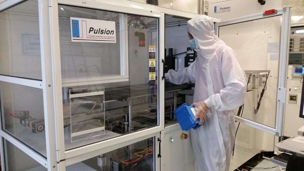
The new energy technologies and nanomaterials (Liten) branch of the French Alternative Energies and Atomic Energy Commission claims to have developed an indium-free monocrystalline solar cell based on passivated contacts with a 22.4% efficiency.
The scientists explained that the device was built with a new cell architecture, named CARLAH, which is based on what they called a “high-temperature heterojunction” approach. The special architecture is created by combining ultra-thin polycrystalline silicon layers, with a thickness of up to 20 nm, with films of passivated transparent conductive oxide (TCO) contacts.
“Our teams have designed a simplified processing method that generates strong ‘external getter' effects (extraction of metallic impurities) suitable for low-cost crystalline silicon (c-Si) substrates with a low carbon footprint,” the research institute specified. “The structures created are, moreover, compatible with integration in Perovskites/c-Si tandem cells.”
The French research group stated that passivated contacts for solar cells are commonly fabricated with tin-doped indium oxide (ITO), which has high costs due to the limited availability of indium. “In order to improve the economical balance and environmental footprint of this type of cell, the ITO layers usually used on the front panel have been compared by our laboratories with Zinc (AZO) based layers on single junction structures,” it further explained. “Like ITO, the AZO layers studied here are deposited by physical vapor deposition (PVD), a process that facilitates their transfer to industry.”
The solar cell was built in industrial format (M2) and its efficiency is currently a world record for this type of cell on an industrial scale, the researchers said.
Liten achieved a 24.25% peak efficiency for a silicon heterojunction solar cell in December 2019. The cell developers said at the time they were able to increase performance by improving the plasma-enhanced chemical vapor deposition of amorphous silicon nanolayers and the conductive and anti-reflective transparent oxide layers. They also reduced wafer-handling damage during manufacturing.
This content is protected by copyright and may not be reused. If you want to cooperate with us and would like to reuse some of our content, please contact: editors@pv-magazine.com.


By submitting this form you agree to pv magazine using your data for the purposes of publishing your comment.
Your personal data will only be disclosed or otherwise transmitted to third parties for the purposes of spam filtering or if this is necessary for technical maintenance of the website. Any other transfer to third parties will not take place unless this is justified on the basis of applicable data protection regulations or if pv magazine is legally obliged to do so.
You may revoke this consent at any time with effect for the future, in which case your personal data will be deleted immediately. Otherwise, your data will be deleted if pv magazine has processed your request or the purpose of data storage is fulfilled.
Further information on data privacy can be found in our Data Protection Policy.