A French-Canadian research group and CPV specialist Stace have fabricated a triple-junction concentrator photovoltaic (CPV) module encapsulated with a polydimethylsiloxane (PDMS) layer based on silica beads. The novelty of their approach consists in controlling the deposition of the silica beads through an additional manufacturing step, in which the microbeads are submerged into PDMS.
According to the researchers, the concept is compatible with high-volume manufacturing. “We haven’t estimated the cost for the cell since the supply chain is not fully available yet, so we cannot give an exact number of the extra cost of the microbeads layer,” Maxime Darnon, from the Laboratory of Nanotechnologies and Nanosystems, told pv magazine. “However, it is an add-on process in the manufacturing of CPV modules, therefore there is no need to fully redevelop the CPV module fabrication line, but just to add one step in the line.”
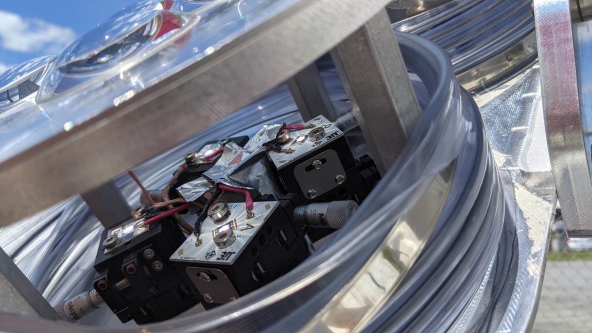
The CPV module relies on a 50 x 50 mm2 silicone-on-glass (SoG) Fresnel lens that concentrates direct sunlight onto hexagonally shaped high-efficiency triple-junction solar cells measuring 3 mm in width and built with three different III-V materials: indium gallium phosphide (InGaP) for the first junction; gallium-indium-arsenide (GaInAs) for the second element; and germanium for the third unit.
The researchers explained that PDMS is commonly utilized as a protective layer in CPV cells and added it also induces parasitic reflections at its interface with the air, which reduces light absorption. They minimized the reflection caused by this layer through the incorporation of a microstructured ARC consisting of a monolayer of silica beads submerged by around 25% into the PDMS layer itself.
The PDMS layer was spin-coated on the cells at a spin rate of 6,000 revolutions per minute for 120 seconds to obtain a thickness of around 6 micrometers, which the research group describes as having negligible effects on the optical performance of the device. The hexagonally close-packed silica beads were deposited on the PDM via a fluid flow process through which the beads are first placed on an easy-to-handle substrate and then moved onto the PDMS surface, which was developed by the French Alternative Energies and Atomic Energy Commission (CEA).
The CPV module developed with the new manufacturing process showed a short-circuit current that was up to 3.7% higher than that of a reference module. A series of simulations conducted by the group has also shown that this improvement may reach 4.8% with beads with a smaller diameter and a submergence degree of around 60%. “The microbeads have demonstrated their ability to lower the Fresnel reflection losses by providing a smooth optical transition from air to PDMS over a wide angular range,” it concluded.
The manufacturing process is described in full in the study “Microstructured antireflective encapsulant on concentrator solar cells,” published in Progress in Photovoltaics.
This content is protected by copyright and may not be reused. If you want to cooperate with us and would like to reuse some of our content, please contact: editors@pv-magazine.com.


By submitting this form you agree to pv magazine using your data for the purposes of publishing your comment.
Your personal data will only be disclosed or otherwise transmitted to third parties for the purposes of spam filtering or if this is necessary for technical maintenance of the website. Any other transfer to third parties will not take place unless this is justified on the basis of applicable data protection regulations or if pv magazine is legally obliged to do so.
You may revoke this consent at any time with effect for the future, in which case your personal data will be deleted immediately. Otherwise, your data will be deleted if pv magazine has processed your request or the purpose of data storage is fulfilled.
Further information on data privacy can be found in our Data Protection Policy.