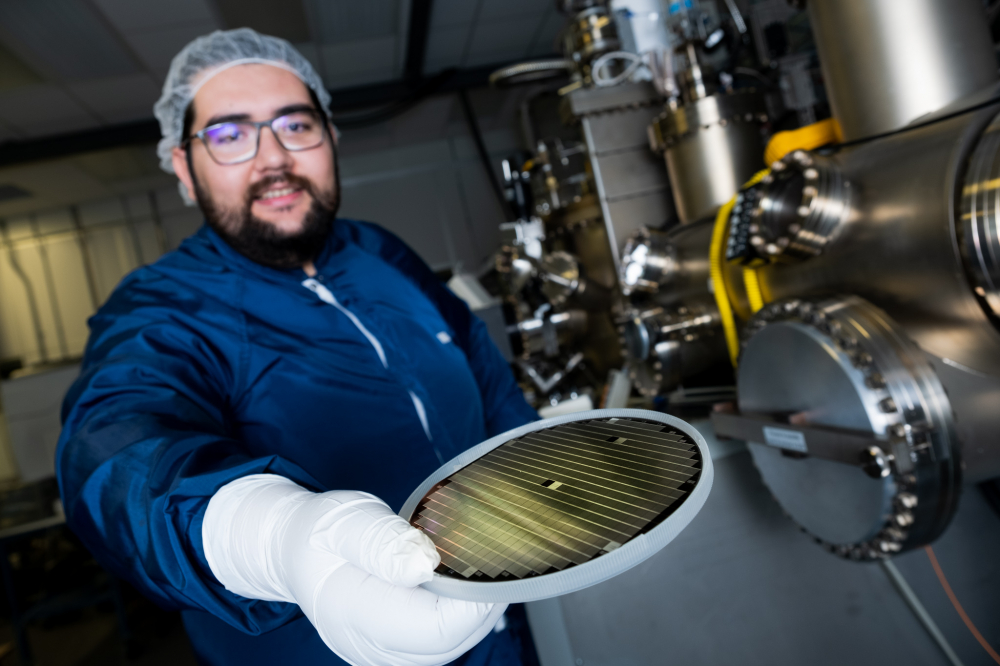
A research team from Canada’s Sheerbroke University says it has created a nanoporous germanium-based (np-Ge) material which could improve the efficiency of multi-junction solar cells based on III-V elements such as gallium arsenide.
In the paper Uprooting defects to enable high-performance III–V optoelectronic devices on silicon, published in Nature, the scientists said their approach was based on reducing to a minimum the use of germanium – the availability of which is very limited compared to silicon – on a high-performance epitaxial device they developed to be integrated into solar cells and other semiconductor devices.
The researchers deposited a 2μm layer of germanium – 100 times less than the thickness of a sheet of paper – on a mechanical support to absorb light. They described the process as a significant scientific and technological challenge due to the small size of the device and, in particular, to the defects caused by the deposition process which are said to lower solar cell performance.
Two-step process
The scientists reportedly found a way to suppress threading dislocations on the surface of the np-Ge material by using dislocation-selective electrochemical deep etching followed by thermal annealing.
The two-step process, said the researchers, creates nanovoids which attract undesirable dislocations, facilitating their subsequent annihilation. “Devices like photodetectors, multi-junction solar cells, microprocessors [and] modulators, based on Ge-on-Si [germanium on silicon] technology must tackle these issues in order to achieve industry standards,” the study noted.
Cathodoluminescence measurements showed the process creates nanovoids which increase the recombination probabilities of threading dislocations, drastically reducing their presence in the engineered germanium layer. “Nanovoids are formed in the Ge layer as well as in the Si substrate by electrochemical porosification, followed by thermal annealing, creating a new configuration referred to as nanovoid-based Ge/Si virtual substrate,” the paper stated.
Cost reduction
Previous techniques used to eliminate threading dislocation density, the scientists said, were limited to small-scale processes and require the use of expensive and complex technologies. “The cost reduction per solar cell can be as high as 75% when the much lower prices and larger areas of Si wafers are considered,” they wrote.
Research into germanium for solar has re-emerged with several projects announced in the last two years.
Innovations include a method of producing gallium arsenide solar cells with a reusable germanium substrate developed by scientists at the U.S. National Renewable Energy Laboratory and the Korea Advanced Institute of Science and Technology; and an ultra-thin solar cell based on gallium arsenide built by a research team from Germany’s Fraunhofer ISE and France’s Center for Nanoscience and Nanotechnology.
The cost of producing solar cells based on compounds of III-V element materials – named according to the groups of the periodic table they belong to – has confined such devices to niche applications including drones and satellites, where low weight and high efficiency are more pressing concerns than cost, in relation to the energy produced.
This content is protected by copyright and may not be reused. If you want to cooperate with us and would like to reuse some of our content, please contact: editors@pv-magazine.com.


By submitting this form you agree to pv magazine using your data for the purposes of publishing your comment.
Your personal data will only be disclosed or otherwise transmitted to third parties for the purposes of spam filtering or if this is necessary for technical maintenance of the website. Any other transfer to third parties will not take place unless this is justified on the basis of applicable data protection regulations or if pv magazine is legally obliged to do so.
You may revoke this consent at any time with effect for the future, in which case your personal data will be deleted immediately. Otherwise, your data will be deleted if pv magazine has processed your request or the purpose of data storage is fulfilled.
Further information on data privacy can be found in our Data Protection Policy.