While plenty in the solar industry warn that more work on the fundamentals of perovskite solar cells is needed before they can move to commercialization, others are forging ahead with the development and testing of processes compatible with large-scale production.
One such customer in the United States recently took delivery of an atomic layer deposition (ALD) tool from Dutch supplier SALD. According to SALD, the unnamed customer plans to use the tool in a pilot production line for perovskite solar cells.
Little else is known about the buyer or its plans for perovskite solar cell production. However, SALD CTO Erik Kremers told pv magazine that its atomic layer deposition equipment could fulfil a number of roles on such a production line.
“A typical application for ALD would be TiO2 [titanium oxide] or SnO2 [tin oxide] buffer layers inside the electron contact,” he said. “Other applications are ZnO:Al for tunnel recombination layers and transparent conductive oxides.”
The announcement makes note of the tool’s suitability for “roll to roll” processes with flexible substrate materials, but Kremers also noted that it could also be suitable for deposition on to glass, or even silicon to create a tandem cell structure.
Tin-based perovskite
SALD also makes mention of tin-based perovskites, which have been less researched and only achieved significantly lower performances than their lead-based counterparts. There is still interested in tin-based materials, as these avoid the use of lead which is toxic to humans and can cause problems if it finds its way out of the cell and into the environment.
“While it is possible to replace lead with tin, tin gradually oxidizes, causing the perovskite's crystalline structure to be lost,” said Kremers. “It is precisely this oxidation that is to be prevented by the use of SALD technology in order to ensure long-term stability.”
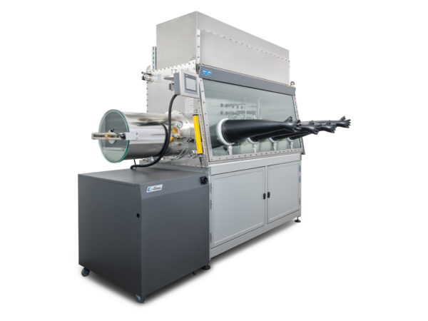
Image:SALD
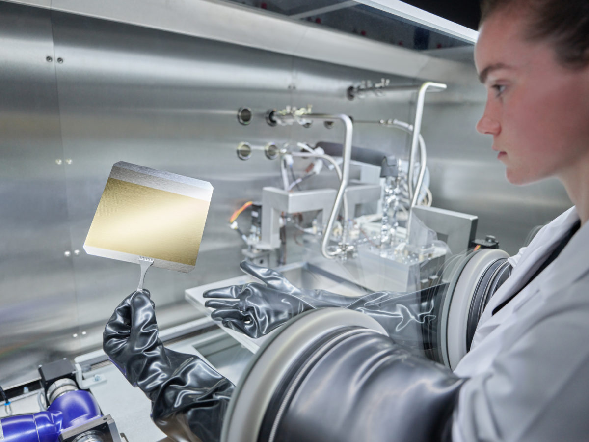
The tool consists of a glove box, and allows for cells to be processed in a nitrogen atmosphere, protecting the sensitive layers from ambient air, before the protective layer is deposited on top. It can process two M6 wafers at once, according to Kremers.
“The deposition rate is 1 nanometer per second and throughput depends on the layer thickness. A rough indication for the throughput at 10 nm layer thickness is approximately 100 wafers per hour.”
PVD alternative
At these rates, far from the several thousand wafer per hour processed in commercial silicon cell production, it’s likely that the customer will be experimenting with different possibilities for larger-scale processing, and Kremers is also keen to point out that even at this scale, its spatial ALD technology is “easily up-scalable to high volume production with a low cost of ownership.”
Another option being investigated for likely similar functions in future perovskite cell manufacturing is physical vapor deposition (PVD), a process type already used in various functions for silicon cell manufacturing. Here though, Kremers noted several advantages for SALD’s atomic layer deposition technology.
“ALD does not induce sputter damage to the sensitive perovskite material. Moreover, it results in dense layers that are well-suited as moisture permeation barrier, which can enhance the stability of the perovskite,” he explained. “Spatial ALD in comparison to PVD processes show that for the same functionality the layers thickness is less, so less material is necessary. This benefits in lower costs per m² and higher throughput.”
This content is protected by copyright and may not be reused. If you want to cooperate with us and would like to reuse some of our content, please contact: editors@pv-magazine.com.


By submitting this form you agree to pv magazine using your data for the purposes of publishing your comment.
Your personal data will only be disclosed or otherwise transmitted to third parties for the purposes of spam filtering or if this is necessary for technical maintenance of the website. Any other transfer to third parties will not take place unless this is justified on the basis of applicable data protection regulations or if pv magazine is legally obliged to do so.
You may revoke this consent at any time with effect for the future, in which case your personal data will be deleted immediately. Otherwise, your data will be deleted if pv magazine has processed your request or the purpose of data storage is fulfilled.
Further information on data privacy can be found in our Data Protection Policy.