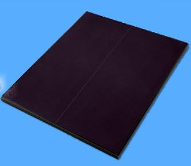
Japanese chemical company Kaneka has designed a two-terminal (2T) perovskite-crystalline tandem solar cell using a 145 μm thick industrial Czochralski (CZ) silicon wafer.
The company's researchers built the cell with an anti-reflection intermediate layer relying on what they call “gentle textured structures” that were applied on the front side of the bottom. This reportedly enables a significant improvement in the typical light confinement effects in perovskite-silicon tandem devices.
“Light management technology is mandatory to fully utilize the wide range of the solar spectrum in a solar cell, especially for a 2T tandem structure, since its top and bottom cells are electrically connected in series and required to satisfy the constraints of current matching whereby the respective currents at the operating point are aligned to some extent,” they said. “Because of the large difference in the refractive indices between perovskite and crystalline silicon (c-Si) materials, the optimized intermediate layer as shown acts as an anti-reflection coating to suppress the reflection loss of the infrared light that is utilized in the bottom cell.”
The tandem device achieved a power conversion efficiency of 29.2%, an open-circuit voltage of 1.929 V, a short-circuit current density of 19.5 mA cm−2, and a fill factor of 77.55%. The result, which was confirmed by Fraunhofer ISE Callab, improves on the 28.3% efficiency Kaneka had previously achieved for a device with the same architecture, withe the main differences being the passivation layer and wafer thickness.
“This is the highest certified power conversion efficiency of 2T perovskite-silicon tandem solar cells using CZ wafer to our knowledge,” the company said, noting that they are currently considering moving to a four-terminal (T4) configuration for the further development of the device.
The company presented the new cell in “High efficiency perovskite/heterojunction crystalline silicon tandem solar cells: towards industrial-sized cell and module,” which was recently published in the Japanese Journal of Applied Physics.
Kanela has developed in the past what is still the second most efficient solar cell based on crystalline silicon – a 26.63%-efficient crystalline silicon solar cell featuring heterojunction and back-contact technology.
*The headline of the article was updated to reflect that the cell is a T2 device and not a T4 cell, as we previously reported.
This content is protected by copyright and may not be reused. If you want to cooperate with us and would like to reuse some of our content, please contact: editors@pv-magazine.com.


1 comment
By submitting this form you agree to pv magazine using your data for the purposes of publishing your comment.
Your personal data will only be disclosed or otherwise transmitted to third parties for the purposes of spam filtering or if this is necessary for technical maintenance of the website. Any other transfer to third parties will not take place unless this is justified on the basis of applicable data protection regulations or if pv magazine is legally obliged to do so.
You may revoke this consent at any time with effect for the future, in which case your personal data will be deleted immediately. Otherwise, your data will be deleted if pv magazine has processed your request or the purpose of data storage is fulfilled.
Further information on data privacy can be found in our Data Protection Policy.