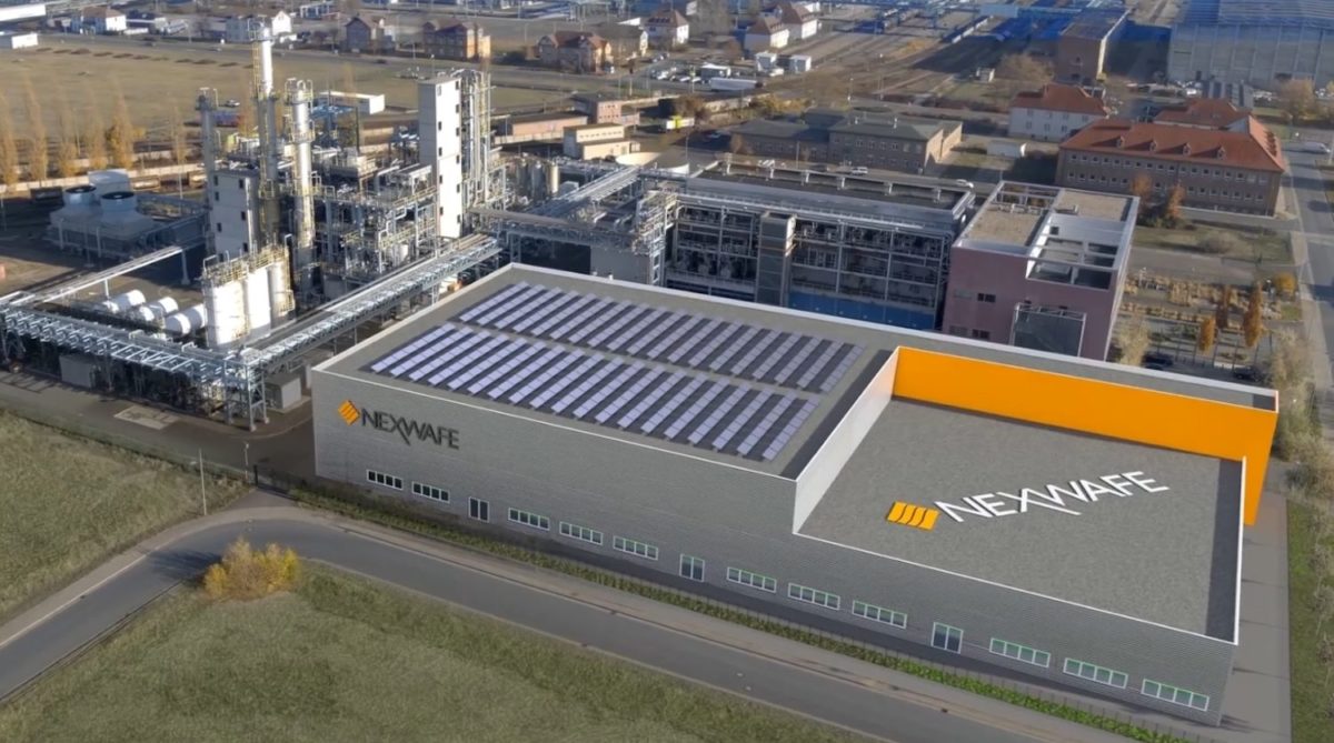
German wafer manufacturer NexWafe GmbH announced it secured financing of €30 million ($32.0 million) from current and new investors.
The company said it will use the funds to move forward with the construction of its planned wafer factory in Bitterfeld, in the district of Anhalt-Bitterfeld, Saxony-Anhalt, Germany.
“The funds come from NexWafe’s current group of investors, including Reliance New Energy Limited, Aramco Ventures and Athos Venture GmbH, as well as new investors, including the Honorable Malcolm Turnbull AC and Keshik Capital, led by Alex Turnbull,” the company said, noting that it intends to raise additional funds in the second half of this year.
The wafer manufacturer also announced a plan to build a new manufacturing facility in Saudi Arabia with the support of the country's Sustainability Fund and Aramco Ventures, the investment arm of Saudi oil group Aramco.
“NexWafe’s process supports urgent U.S. and European efforts to re-shore domestic solar wafer manufacturing and cell production by increasing supply-chain sourcing diversity and resilience,” the company stated, without providing more details on the Saudi project.
In October 2021, Reliance New Energy Solar Limited (RNESL), an arm of Mukesh Ambani-led Reliance Industries Limited, invested €25 million in NexWafe.
The manufacturer claims that its EpiWafers technology could help module producers to achieve dramatically higher degrees of efficiency, without having to upgrade their production lines. It also claims that its technology can enable the production of ultra-thin wafers. It has already demonstrated this on its pilot line in Freiburg, Germany. In addition to ultra-thin wafers, Nexwafe plans to use tandem architectures in the future.
NexWafe develops and produces monocrystalline silicon wafers grown directly from inexpensive raw materials. The continuous, direct gas-to-wafer manufacturing process obviates the need for costly and energy-intensive intermediate steps such as polysilicon production and ingot pulling on which traditional wafer manufacturing relies. The process also reportedly minimizes wastage, cutting wafer production costs by up to 30%. It also offers a 70% reduction in carbon dioxide emissions during manufacturing, according to the company.
This content is protected by copyright and may not be reused. If you want to cooperate with us and would like to reuse some of our content, please contact: editors@pv-magazine.com.


1 comment
By submitting this form you agree to pv magazine using your data for the purposes of publishing your comment.
Your personal data will only be disclosed or otherwise transmitted to third parties for the purposes of spam filtering or if this is necessary for technical maintenance of the website. Any other transfer to third parties will not take place unless this is justified on the basis of applicable data protection regulations or if pv magazine is legally obliged to do so.
You may revoke this consent at any time with effect for the future, in which case your personal data will be deleted immediately. Otherwise, your data will be deleted if pv magazine has processed your request or the purpose of data storage is fulfilled.
Further information on data privacy can be found in our Data Protection Policy.