An international research team has sought to apply black silicon (bSi) to develop ultra-thin substrates for applications in interdigitated back-contact (IBC) solar cells.
This kind of silicon offers the advantage of enabling the production of ultrathin and flexible wafers with lower impurity levels, which result in exceptional light-absorbing properties and low production costs. “Black silicon is a random nanotexture that reduces surface reflectance from all directions to a minimum, so that Si becomes black to the naked eye as opposed to conventional micron-scale random pyramids,” the scientists explained.
Image: Universitat Politècnica de Catalunya, Nano-Micro Small, Creative Commons License CC BY 4.0
They used deep reactive ion etching (DRIE) at cryogenic temperatures to produce Si substrates with different thicknesses down to 10 µm. This process is a plasma-based etching technique that yields deep holes and trenches with steep sides in silicon wafers.
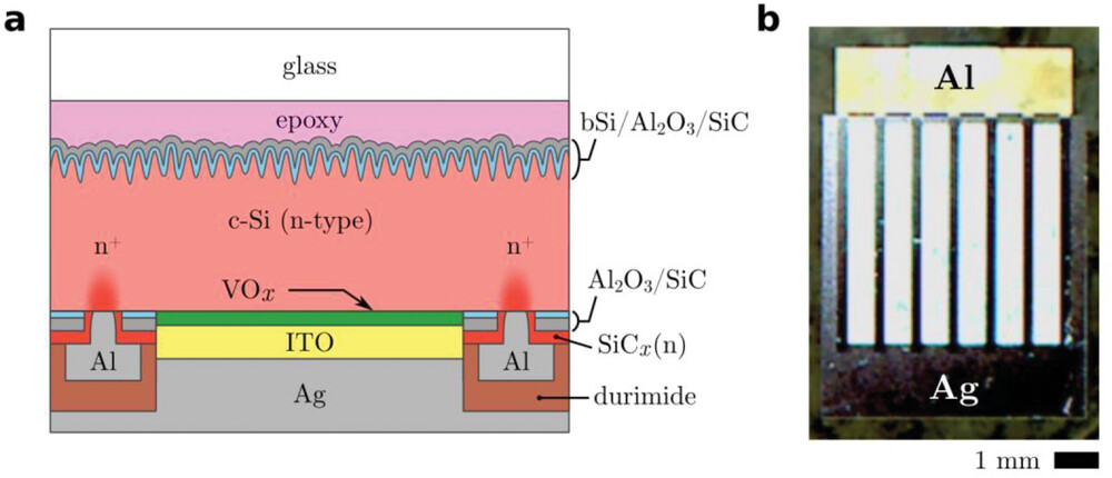
The researchers utilized a Si substrate with a thickness of 40 µm to build a solar cell with IBC architecture, which they said can exploit the optical advantage of a bSi front surface in the material. “The IBC c-Si solar cell structure used is based on vanadium oxide (VOx) and laser processed phosphorus-doped silicon carbide stacks as hole and electron transport layers, respectively,” they explained.
The cells were also relying on a surface passivation layer made of aluminum oxide (Al2O3) and silicon carbide (SiC). “We chose a conformal Al2O3 layer deposited by atomic layer deposition (ALD) as it offers excellent surface passivation of bSi nanotexture, achieving average lifetimes above 250 µm in our bSi ultra-thin wafers,” the scientists said.
Popular content
The PV device achieved a power conversion efficiency of 16.4%, an open-circuit voltage of 633 mV, a short-circuit current density of 35.4 mA cm−2 , and a fill factor of 73.4%. For comparison, a reference cell with a polished front surface and without the black silicon wafer achieved an efficiency of 11.5%, an open-circuit voltage of 600 mV, a short-circuit current density of 27.1 mA cm−2, and a fill factor of 70.7%.
“External Quantum Efficiency (EQE) results with bSi front surface improve the identical device with a polished front surface in all the measured spectrum ranges, from near-infrared (NIR) to ultraviolet (UV), demonstrating that the optical properties can be successfully transferred to electrical photovoltaic performance in a final, encapsulated, cell,” the scientists concluded, noting that further work is needed to improve light-trapping effectiveness of the front bSi texture.
They presented the new wafer and cell technology in the paper “Black Ultra-Thin Crystalline Silicon Wafers Reach the 4n2 Absorption Limit–Application to IBC Solar Cells,” published in Nano-Micro Small. The research group includes academics from the Universitat Politècnica de Catalunya in Spain and the Aalto University in Finland.
This content is protected by copyright and may not be reused. If you want to cooperate with us and would like to reuse some of our content, please contact: editors@pv-magazine.com.


By submitting this form you agree to pv magazine using your data for the purposes of publishing your comment.
Your personal data will only be disclosed or otherwise transmitted to third parties for the purposes of spam filtering or if this is necessary for technical maintenance of the website. Any other transfer to third parties will not take place unless this is justified on the basis of applicable data protection regulations or if pv magazine is legally obliged to do so.
You may revoke this consent at any time with effect for the future, in which case your personal data will be deleted immediately. Otherwise, your data will be deleted if pv magazine has processed your request or the purpose of data storage is fulfilled.
Further information on data privacy can be found in our Data Protection Policy.