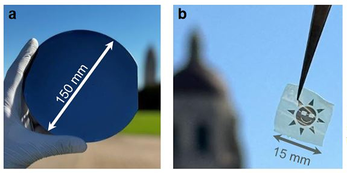
A group of researchers led by Stanford University and Belgian research center Imec has developed a new manufacturing process to build transition metal dichalcogenide (TMD) solar cells in a scalable fashion, thus bringing them closer to commercial production.
TMDs are two-dimensional materials with remarkable semiconducting properties and high optical absorption coefficients. This makes them suitable for the production of semi-transparent and flexible solar cells with potential applications in aerospace, architecture, electric vehicles, and wearable electronics, where light weight, a high power-per-weight ratio, and flexibility are very desirable.
“We have developed a scalable, mass production-friendly method which yields photovoltaic-grade, wafer-scale tungsten diselenide (WSe2) films with a layered van der Waals structure and superior characteristics, including charge carrier lifetimes up to 144 ns, over 14 times higher than those of any other large-area TMD films previously demonstrated,” the research's co-lead author, Koosha Nassiri Nazif, told pv magazine.
The group designed a sputtered multilayer WSe2 film with a thickness of 15−30 nm for applications on on a 150 mm wafer via a selenization process based on either a solid-source selenium (SS-Se) at 900 C or low-thermal-budget hydrogen selenied (H2Se) precursors at 650 C. The resulting WSe2 film had an energy bandgap of 1.2 eV to 1.3 eV, which the scientists described as near-ideal for solar energy harvesting.
The film reportedly shows superior characteristics compared to previous selenization reports, as well as smooth and uniform surfaces. According to the researchers, with improved contacts and doping, it could reach an efficiency of up to 22.3% in an optimized solar cell design.
“Our realistic models show that such carrier lifetimes correspond to around 22% power conversion efficiency and around 64 W g–1 specific power in a packaged solar cell, or approximately 3 W g–1 in a fully packaged solar module. The results of this study could facilitate the mass production of high-efficiency multilayer WSe2 solar cells at low cost,” Nassiri Nazif stated.
The novel cell concept was described in the paper “Toward Mass Production of Transition Metal Dichalcogenide Solar Cells: Scalable Growth of Photovoltaic-Grade Multilayer WSe2 by Tungsten Selenization,” which was recently published in ACS Nano. The research team included academics from the University of Colorado Boulder and the US Department of Energy's National Renewable Energy Laboratory (NREL), as well as from Hasselt University and the University of Antwerp in Belgium,
This content is protected by copyright and may not be reused. If you want to cooperate with us and would like to reuse some of our content, please contact: editors@pv-magazine.com.


By submitting this form you agree to pv magazine using your data for the purposes of publishing your comment.
Your personal data will only be disclosed or otherwise transmitted to third parties for the purposes of spam filtering or if this is necessary for technical maintenance of the website. Any other transfer to third parties will not take place unless this is justified on the basis of applicable data protection regulations or if pv magazine is legally obliged to do so.
You may revoke this consent at any time with effect for the future, in which case your personal data will be deleted immediately. Otherwise, your data will be deleted if pv magazine has processed your request or the purpose of data storage is fulfilled.
Further information on data privacy can be found in our Data Protection Policy.