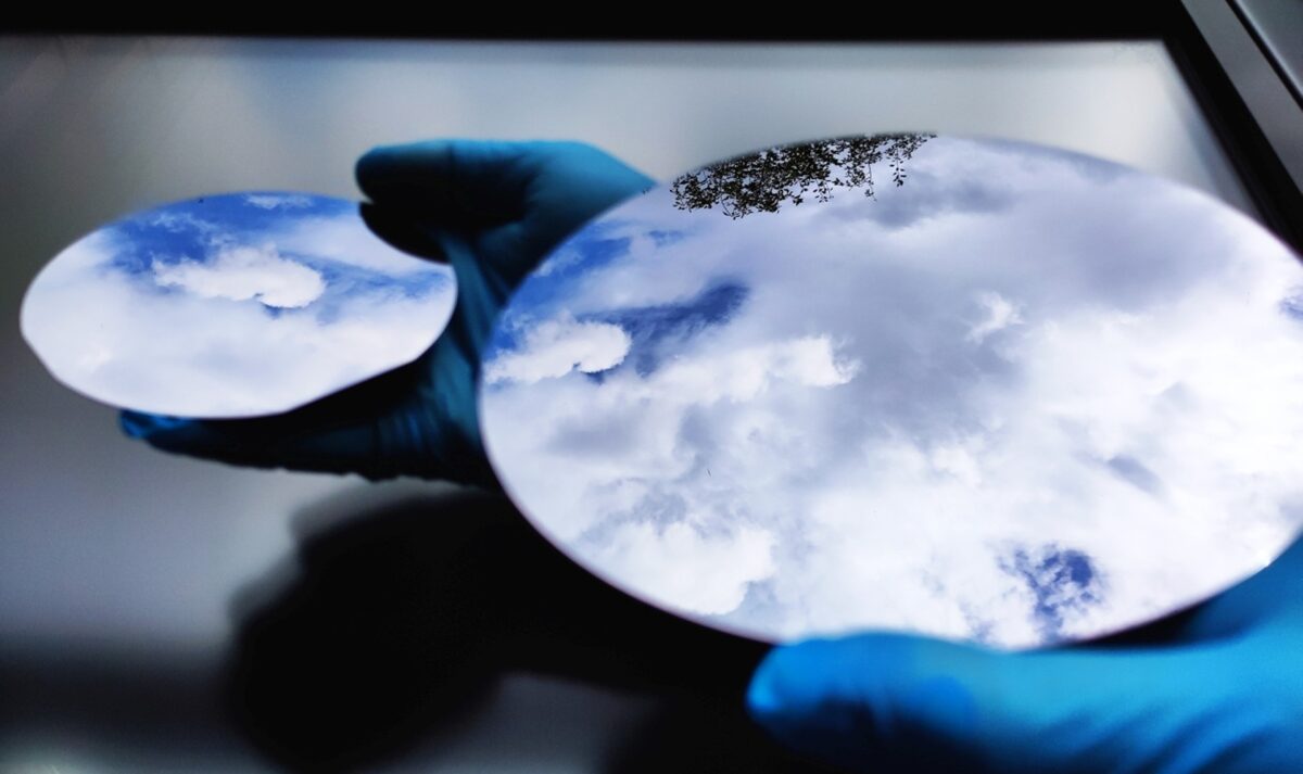
Scientists at the Fraunhofer Institute for Solar Energy Systems ISE have produced indium phosphide on InP-on-GaAs wafers up to 150 mm in diameter.
Working in collaboration with German semiconductor specialists III/V-Reclaim, the team developed a process to deposit a thin layer of high-quality indium phosphide on gallium arsenide.
The team said the application is challenging because defects occur during the growth of the indium phosphide, which can degrade the performance of the final device. To avoid such defects, the team incorporated a series of so-called ‘metamorphic buffer layers' and by subjecting the fully grown InP-on-GaAs wafer to a special chemical-mechanical polishing step.
Following the surface treatment, the wafers are shiny and feature very low surface roughness and defect densities below 5*106 cm-2. Fraunhofer ISE said in a statement that their new wafers can “effectively replace classic indium phosphide in a variety of applications, offering a scalable pathway to lower cost.”
Carmine Pellegrino, project manager at Fraunhofer ISE, said companies can use the InP-on-GaAs substrates to manufacture high-efficiency devices.
“However, it costs much less than InP and there are no limitations in terms of scalability to even 8-inch diameter wafers,” added Pellegrino.
The research team have tested the material quality and performance of the wafers against standard indium phosphide substrates and say the results have been “extremely promising.”
“Photovoltaic cells fabricated on our engineered wafers achieve open-circuit voltages comparable to reference devices on prime InP wafers,” Pellegrino said. “The performance is consistently uniform across the entire 6-inch wafer, enabling reliable, high-yield production.”
Pellegrino noted that the production costs of the new substrates are significantly lower than those of indium phosphide wafers, with potential savings potential up to 80% in mass production.
“In addition, our approach bypasses constraints on the supply of indium phosphide,” said Pellegrino.
This content is protected by copyright and may not be reused. If you want to cooperate with us and would like to reuse some of our content, please contact: editors@pv-magazine.com.


By submitting this form you agree to pv magazine using your data for the purposes of publishing your comment.
Your personal data will only be disclosed or otherwise transmitted to third parties for the purposes of spam filtering or if this is necessary for technical maintenance of the website. Any other transfer to third parties will not take place unless this is justified on the basis of applicable data protection regulations or if pv magazine is legally obliged to do so.
You may revoke this consent at any time with effect for the future, in which case your personal data will be deleted immediately. Otherwise, your data will be deleted if pv magazine has processed your request or the purpose of data storage is fulfilled.
Further information on data privacy can be found in our Data Protection Policy.