Researchers from the University of Central Florida in the United States have developed a photonic curing technique that reportedly improves the copper (Cu) metallization of solar cells by reducing Cu oxidation.
“We have already advanced to achieving cell efficiencies close to 20% with copper metallization, and we are actively addressing oxidation and other integration challenges to move closer to industry adoption,” the research's corresponding author, Prasanth Kumar, told pv magazine. “Our work was funded by the U.S. Department of Energy (DOE).”
Photonic curing is a high-temperature technique that uses intense bursts of light from flash lamps to rapidly heat the surface of a material. This approach can “cure” metals or inks without overheating or damaging the underlying layers, making it particularly useful in electronics and solar cell manufacturing to improve conductivity and material quality.
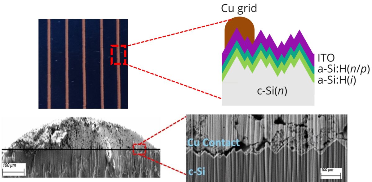
In their work, the scientists treated Cu micro- and nanoparticles with laser sintering to generate rapid, localized heating via a high-intensity laser beam. This method reportedly allows Cu pastes to be cured on temperature-sensitive substrates without causing thermal stress.
“The laser sintering technique enables selective energy absorption, reducing substrate damage and enhancing adhesion between the Cu and indium tin oxide (ITO) layers compared to conventional sintering methods,” the scientists explained. “Additionally, the photonic curing process is scalable and compatible with high-volume photovoltaic manufacturing.”
For the experiments, Cu micro- and nanoparticles were deposited onto 140 μm-thick, ITO-coated Czochralski (Cz) wafers using a microdispensing system, while sintering was performed with a CO₂ laser. A commercial copper paste supplied by U.S.-based printed electronics manufacturer Novacentrix was used for high-resolution printing.

Image: Image: University of Central Florida
Using scanning electron microscopy (SEM), energy-dispersive X-ray spectroscopy (EDAX), and profilometry, the team analyzed Cu line resistance, bulk resistivity, and contact resistivity at the ITO/Cu interface. They found that the process produced a dense, compact Cu layer with reduced porosity and strong adhesion of Cu contacts.
Under “optimized” conditions, the process achieved a bulk resistivity of approximately 19 μΩ·cm and a contact resistivity of around 35 mΩ·cm². The researchers noted that these values are low enough to enable significant reductions in Cu consumption, offering a viable path toward cost-effective and reliable metallization processes.
“Contacts formed with line widths of 150–200 μm in this work achieve high aspect ratios in the range of 0.1 to 0.15,” the team said. “Future efforts will focus on reducing the line widths of the contact fingers and increasing the aspect ratio, which is particularly important for minimizing optical shading losses.”
Looking ahead, the researchers plan to investigate the thermal interactions that occur during laser sintering of Cu paste, aiming to further optimize the process for next-generation solar cell manufacturing.
The novel technique was presented in the paper “Photonic Curing of Copper Inks: A Pathway to Scalable Copper Metallization for Solar Cells,” published in physica status solidi (PSS). The research team included academics from the University of Delaware.
This content is protected by copyright and may not be reused. If you want to cooperate with us and would like to reuse some of our content, please contact: editors@pv-magazine.com.


It seems like if you are try to ink press copper conductors and make them really fine researchers try to find a thin tube for printing next gen capacitors found that the probisia from the Egypt mosquito not only gave the smallest tube diameter and also the most durable for inkjet printer nib they valued the probisia at one dollar each for the time it took to harvest them