U.S.-based inspection equipment manufacturer Brightspot Automation has launched Plus-Spot, a non-contact photoluminescence (PL) imaging tool to reveal defects, such as cell cracks, thin-film shunts in panels, and other non-uniformities. It is suitable for quality control in silicon, thin film, and III-V multijunction space cell manufacturing applications, supporting devices that range in size from mini-module to conventional utility-scale panels.
The new Plus-Spot tool supports off-line and in-line quality control processing, as well as pre-installation quality control, and research and development activity. The panels can be partially processed or finished, according to the company.
As a non-invasive or non-contact system, it detects defects and non-uniformities quickly without cabling. “Standard capabilities include single-intensity PL imaging, intensity-stepped PL imaging, and time series imaging,” a company spokesperson told pv magazine, noting that multispectral imaging with a filter wheel, and electroluminescence (EL) imaging are also supported.
In addition, the tool enables biased PL imaging, monochromatic and bichromatic light IV, and dark IV measurements, spot spectral characterization, and rear-side glass crack detection in superstrate cadmium telluride (CdTe) panels.
“Front-side glass cracks in CdTe panels are easily seen in the standard PL images. Successful PL imaging has been confirmed through hazy encapsulant for layup table applications,” said the company's spokesperson.
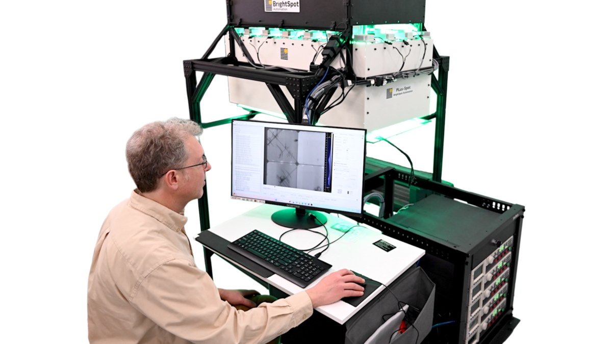
The system’s cameras have resolutions of 20 up to 61 megapixels with customizable filters to match customers’ semiconductor bandgaps. The test area dimensions are also customizable.
The LED arrays are heat-sinked, supporting up to 1 sun intensity, and available in blue or green to match customer applications. Programmable power supplies drive the LED arrays. The arrays are enclosed to eliminate room light artifacts, as well as to improve light intensity and uniformity, according to the company.
Housing is a customized metal frame for integration in a factory transport system or over a table. “The tool can be oriented for sunnyside-up, sunnyside-down, or sunnyside-sideways panel orientations,” said the spokesperson.
It can be used by thin film manufacturers developing products based on perovskites, CdTe, and copper indium gallium selenide (CIGS) to check film quality after each processing step for statistical process control. “For example, imaging can be performed after the perovskite layer deposition step and then again after the electron transport layer step,” noted the spokesperson.
Building-Integrated (BIPV) and vehicle-integrated PV (VIPV) manufacturers who typically buy panels to integrate into finished products, can use it to test incoming devices prior to integration, or to test them after integration.
Another customer group is satellite solar arrays manufacturers who can use the system to inspect purchased panels for cell cracks prior to integration, or to test panels midway through production or to inspect panels after mounting.
Brightspot Automation claims over 200 customers using its PL and EL systems worldwide throughout the PV value chain. Its proprietary IMPEL software reportedly embodies its expertise in detecting defects in EL and PL images and grading these images based on customer requirements.
This content is protected by copyright and may not be reused. If you want to cooperate with us and would like to reuse some of our content, please contact: editors@pv-magazine.com.


By submitting this form you agree to pv magazine using your data for the purposes of publishing your comment.
Your personal data will only be disclosed or otherwise transmitted to third parties for the purposes of spam filtering or if this is necessary for technical maintenance of the website. Any other transfer to third parties will not take place unless this is justified on the basis of applicable data protection regulations or if pv magazine is legally obliged to do so.
You may revoke this consent at any time with effect for the future, in which case your personal data will be deleted immediately. Otherwise, your data will be deleted if pv magazine has processed your request or the purpose of data storage is fulfilled.
Further information on data privacy can be found in our Data Protection Policy.