Having secured a further €1.5 million ($1.7 million) in funding – this time from Chemiepark Bitterfeld-Wolfen GmbH (CPG) – Nexwafe GmbH has announced it will set up shop for the production of its epitaxially grown, kerfless silicon wafers in Bitterfeld, Germany. It will be the first such facility in the world, the company says.
CPG invested the €1.5 million in the Fraunhofer ISE spin off as part of a funding round led by Saudi Aramco and Germany's Green Gateway Fund II. Overall, Nexwafe has secured €9.5 million in financing for the commercialization of its kerfless wafers.
In December, Nexwafe CEO Stefan Reber told pv magazine there was “lots of interest” in the company's kerfless wafers, which would help secure financing. Mr. Reber said he saw a big market for the product, due to the “significant” advantages it brings.
Solar valley
Nexwafe will set up the facility next year, in the “solar valley” of Bitterfeld, just outside the German capital, Berlin, which has long been renowned for its connections with the solar industry. Nexwafe will work closely with Silicon Products Bitterfeld (SPB) GmbH & Co. KG – based in the same chemical park.
“We are happy to have found, in CPG and SPB two strong partners who share our vision and are able to give us comprehensive and dynamic support,” said Mr. Reber, a Nexwafe co-founder, in an official statement.
While the initial production capacity will be 250 MW, fellow Nexwafe co-founder Frank Siebke told pv magazine at Intersolar Europe it will be easy to scale activity up at Bitterfeld without large investments in infrastructure.
Cost reductions
Price pressures are high – particularly with China's about-turn on solar expected to drive down the price of PV modules by around a third this year – and the obvious potential for cost reductions is at the wafer level, Nexwafe co-founder Roy Segev told pv magazine in Munich. Wafers make up 40% of the cost of a solar PV module, with 40% accounted for by module production and 20% for manufacturing cells.
Current wafer production techniques waste around half of the material and related energy, said Mr. Segev. However Nexwafe’s process – which involves growing crystalline silicon layers on a seed wafer in an in-line oven – means the wafer can be removed without any kerf loss, to form a self-supporting wafer of any size and thickness. The utilization rate is said to be close to 100%.
Furthermore, Nexwafe produces a “drop-in” wafer, meaning any monocrystalline solar cell producer can integrate the company's wafers into their production, without changes to their set up.
Disruptive
The technology is “cutting edge” and “disruptive” says Mr. Segev, who adds Nexwafe does not intend to sell its patented equipment to other companies, and will stick to selling wafers.
Both Mr. Segev and Mr. Siebke are keen to emphasize production will be kept in Germany, while the end product will not only add 0.6% more power to modules but will also be of very high quality. Innovation, local and quality are the key words, the co-founders say.
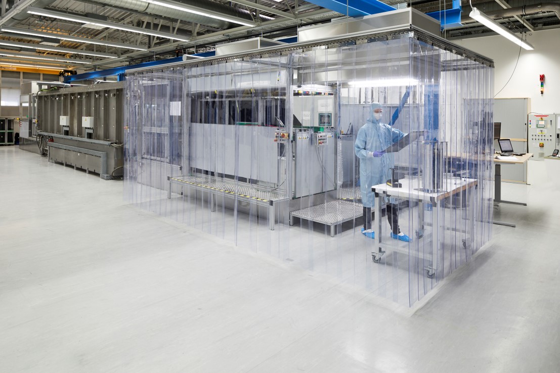
A pilot production facility is being set up in Freiburg, where the Nexwafe headquarters will remain – near the Fraunhofer ISE. The first wafers are expected to be ready towards the end of the year, and will be tested with an unnamed partner.
Several actions still need to be taken, says Mr Siebke, to translate the pilot line to mass production, including upgrading equipment. “We have the blueprint of the equipment we need, however,” he says.
This content is protected by copyright and may not be reused. If you want to cooperate with us and would like to reuse some of our content, please contact: editors@pv-magazine.com.


By submitting this form you agree to pv magazine using your data for the purposes of publishing your comment.
Your personal data will only be disclosed or otherwise transmitted to third parties for the purposes of spam filtering or if this is necessary for technical maintenance of the website. Any other transfer to third parties will not take place unless this is justified on the basis of applicable data protection regulations or if pv magazine is legally obliged to do so.
You may revoke this consent at any time with effect for the future, in which case your personal data will be deleted immediately. Otherwise, your data will be deleted if pv magazine has processed your request or the purpose of data storage is fulfilled.
Further information on data privacy can be found in our Data Protection Policy.