Researchers working on 3D Photovoltaics at the AMOLF institute at Amsterdam’s Science Park have demonstrated a method which uses an atomic force microscope to electrochemically print patterns at the nano scale.
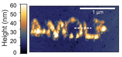
Atomic force microscopy, according to ScienceDirect, is a technique for three-dimensional characterization with a sub-nanometer resolution, and involves the moving of a tiny stylus up and down over a surface. In this application, the stylus – a 50 nanometer platinum needle – moves over the surface “like the needle of a record player”, according to AMOLF. The stylus acts as one electrode, and a small gold plate as another. Both are suspended in a copper sulphate solution, and when voltage is applied, copper is deposited at the precise location of the stylus.
Details of the technique are published in the online journal Nanoscale. AMOLF Ph.D student Mark Aarts was able to use the technique to spell the institution’s name, and he says that he can use the technique to draw “any desired shape on a surface.” And the same technique, the institute says, could be used in the production of a “new generation of nano -architected solar cells.”
Aarts also explained that a curious “double layer” effect discovered during this work could also have implications for the design of batteries or electrocatalysis processes. “A layer with the opposite charge always forms around a charged electrode. This ‘double layer' also forms around our AFM tip and the gold electrode, and that prevents the copper reaction from taking place,” he explains. “the double layer is what facilitates the reaction. By tapping the tip on the surface, the double layer is broken, which allows the reaction to take place locally.”
The researchers describe producing solar cells using this technique as ‘their dream’, and acknowledge that several challenges stand in the way of this becoming a reality. Among these is increasing the height of the nanostructures, and the combination of the nanowires with other material structures needed in a solar cell. “”With electrochemistry, we can easily apply materials simultaneously or in sequence,” said Aarts. “Within the group we are also investigating these processes, and we hope to combine it all in the future.”
This content is protected by copyright and may not be reused. If you want to cooperate with us and would like to reuse some of our content, please contact: editors@pv-magazine.com.


Reminded me of the potential for optical rectennae:
https://en.m.wikipedia.org/wiki/Optical_rectenna