pv magazine: In “Solar Cells and Modules,” which was recently published by Springer, you dedicate a long chapter to amorphous silicon solar cells, which is very much still a niche technology reserved for specific applications. Why hasn't this technology been deployed in rooftop PV arrays?
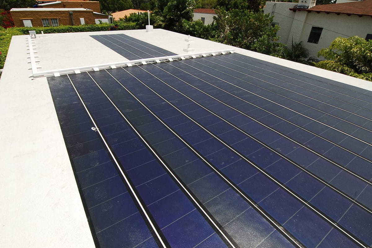
Arvind Shah: The main problem of this technology is the low conversion efficiencies that have so far been attained. Commercially, only about 7 % module stabilized efficiency was reached with a single junction. On a rooftop, space is limited. Therefore, wafer-based crystalline silicon solar modules with over 20% commercial efficiency are preferred.
Hydrogenated amorphous silicon layers are used to manufacture highly efficient heterojunction solar cells, but when they are used for amorphous silicon solar cells, they result in cell efficiencies of just 7%. Are these low efficiencies not sufficiently balanced by lower production costs and simplified manufacturing processes?
Potentially, the production costs of amorphous silicon solar panels could indeed be lower than those of wafer-based crystalline silicon solar modules. But this would only occur once high enough production volumes would be reached. We should take note of the fact that the main factors influencing the production costs of any solar module are the cost of electricity and the investment costs. Now, around 2011, when Chinese manufacturers took over the photovoltaic solar market, they were doing this based on exceedingly low electricity prices, not available anywhere else in the whole world, and interest-free loans from their government. No wonder that they were able to sell solar modules at prices not attainable anywhere else in the whole world.

Image: Brigitte Shah, Wikimedia Commons
With technological improvements and cost reductions, what kind of efficiencies can be reached in the future? What is the maximum theoretical efficiency these cells could reach?
My own institute, the PV Lab Neuchâtel, founded by me in 1984, was in 2011 working in close collaboration with a company called Oerlikon Solar. The latter had attained module efficiencies around 12% for large-area modules, albeit with a much more complicated structure called the Micromorph structure, involving both amorphous silicon and microcrystalline silicon. Oerlikon Solar was not a module producer, but a provider of equipment for manufacturing modules. The companies that made modules with the equipment from Oerlikon Solar had initially a small volume, hence relatively high production costs. These companies were unable to compete in the global market with crystalline silicon moving faster than expected, and they all had to stop activities within a few years. As for the maximum theoretical efficiency these cells may reach, this is a very difficult question. The answer depends on the assumptions you make. If you make realistic assumptions, the limit you can reach is around 16 % for a triple-junction cell. For such a cell, the production costs could be low if you find a way to decrease the cost of equipment and to accelerate the deposition rate of the microcrystalline layer, which are both real challenges.
Amorphous solar cells have big problems with stability and suffer from the “Staebler–Wronski effect” (SWE), which consists of a particular form of light-induced degradation. Is there room for improvement here?
No. During the years 1980 to 2000, there have been numerous attempts to improve the stability of amorphous silicon, by using purer gases, by modifying the deposition parameters, by avoiding/reducing the incorporation of oxygen, iron, and other foreign atoms into the amorphous silicon layer, or by using a totally different deposition process. None of these approaches were successful.
How do amorphous solar cells compare to perovskite solar cells in terms of instability?
It is true that both types of cells suffer from stability problems. However, there are important differences. Amorphous silicon solar cells show initial degradation and their efficiency stabilizes after about two years of normal exposition to sunlight, Furthermore, the decrease in efficiency observed in amorphous silicon is fully reversible – the original state can be recovered through annealing at about 200 C. Moreover, the instability observed in amorphous silicon solar cells depends on their operation temperature – if the latter is high, let's say around 70 C, as commonly encountered in tropical countries, the degradation is much less pronounced. Finally, the degradation in amorphous silicon is a purely physical process, no chemical changes are involved. In contrast with this, we observe for perovskite solar cells that their degradation process, once initiated, apparently continues until the cell is fully degraded. In addition, only a part of the degradation processes observed in today’s perovskite cells during long-term operation is reversible; degradation also depends here on the operation temperature, but it is accelerated, not reduced at higher operation temperatures. Finally, in perovskite cells, the irreversible degradation phenomenon is associated with chemical changes.
In your book, you explain that amorphous silicon does not have a real bandgap. Can you explain what this means?
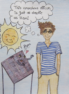
Yes, I can explain this, but a precise explanation will need concepts from solid-state physics, which readers will, in general, be unable to understand. I will therefore attempt to give an intuitive and approximate explanation here. In crystalline semiconductors, there exists a clear bandgap between the upper edge of the valence band and the lower edge of the conduction band. Within this bandgap, there are practically no electronic states at all. In amorphous semiconductors, such as amorphous silicon, what was previously a real bandgap is now a region filled with electronic states such as bandtail states, due to the amorphous, chaotic nature of the material, and midgap states, due to dangling bonds or broken bonds. Therefore, no real bandgap exists in amorphous silicon.
Unlike other solar cells, amorphous silicon cells have a “p-i-n” structure. How does this structure influence their behavior and performance?
The “p-i-n” structure, used for amorphous silicon solar cells, consists mainly of an intrinsic layer. This layer extends over more than 90% of the whole solar cell, whereas the doped layers – the p and n layers – make up less than 10% of the cell. Intrinsic layers of amorphous have a far better quality than doped layers. Furthermore, within the whole i-layer of the p-i-n structure, there exists an internal electric field – a field that helps in transporting and collecting the carriers. All this contributes to obtaining for amorphous silicon solar cells, a reasonable efficiency of about 9-10% efficiency at cell level, whereas with the traditional pn-structure, like those used in all other types of solar cells, one would not attain more than 1%, in the case of amorphous silicon.
The deposition process in the manufacturing of these cells is made mostly through plasma-enhanced chemical vapor deposition (PECVD). Will this process remain the only option for technology developers in the future?
Yes. Many other deposition processes have been tried out. No other process has produced results as good as those obtained with PECVD. At some moment, in the early 2000s, there was a lot of hope for hot-wire deposition. But this process has not created an advantage, although it is at present nevertheless used by some companies for making heterojunction cells.
What kind of improvements are needed in manufacturing processes to open up more commercial possibilities for this technology? How big could this niche become?
Personally, I do not see any improvements here. Japanese and European researchers tried very hard in the early 2000s to find new, alternative materials to be included in multijunction thin-film silicon cells, such as silicon-germanium alloys and special, elaborated forms of silicon-carbon alloys. They did not succeed in finding any viable options.
Do you exclude the possibility that amorphous silicon cells and panels may be used for rooftop or off-grid applications in the future?
No, fundamentally I do not exclude that possibility. However, I very much doubt that anybody will invest massively in this technology today. I will give you here some examples, where amorphous silicon cells and panels would be the ideal choice: windows with selected grades of transparency, greenhouses. Amorphous silicon will also continue to be used for energy scavengers (Internet of Things, watches), because of its high efficiency in indoor conditions and its facility of patterning. Finally, most of the know-how developed for amorphous silicon has now allowed the emergence of valuable and cost-effective manufacturing processes for silicon heterojunction solar cells. My successor, Professor Ballif, who took over as head of the PV Lab in 2005, now concentrates on developing the “solar module of the future,” for the period 2030 to 2040. A module based on a crystalline silicon heterojunction bottom cell and a perovskite top cell. The goal is to reach commercial module efficiencies of 30% at module prices well below €0.30 per watt. In these modules, amorphous interface layers will be a key factor. These modules will constitute a basis for the renaissance of the European photovoltaic industry.
In another interview in this series, Professor Shah spoke to pv magazine about the future of heterojunction PV modules. “Solar Cells and Modules,” published by Springer, was written by Shah and co-author Sylvère Leu. The book includes other contributions from Christophe Ballif, Adinath Funde, Detlef Sontag, Alessandro Romeo, Alessandro Virtuani, Mauro Pravettoni, Urs Muntwyler, and Stefan Nowak.
This content is protected by copyright and may not be reused. If you want to cooperate with us and would like to reuse some of our content, please contact: editors@pv-magazine.com.


The relative inefficiency (in area) may be partially made up in their ability to produce power in cloudy areas, shade, and off-axis.
Hello,
I thought about 6 layer panels. Could that work better for thin film?
I imagine a double output.
Thanks