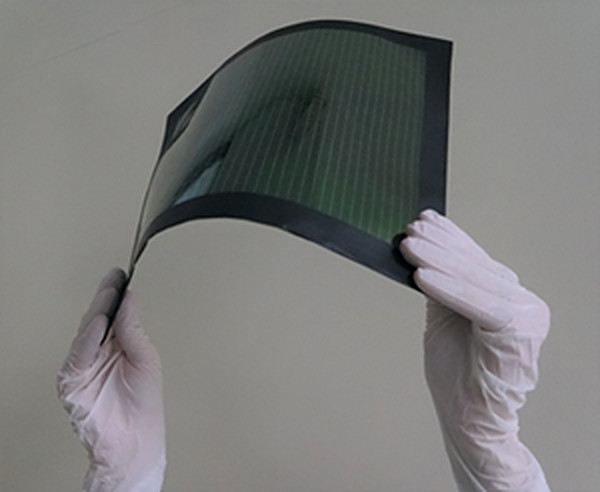
Japanese electronics manufacturer Toshiba has announced a 15.1% power conversion efficiency for a 703cm2 polymer film-based perovskite solar module. The result is claimed to be, by the company, the highest efficiency ever reported for any large, polymer film-based perovskite photovoltaic module to date.
The device was fabricated through a one-step coating method that uses improved ink, film drying processes, and production equipment to form a uniform perovskite layer. The process is said to halve the steps for deposition of the MAPbI3 perovskite layer. The coating speed is said to reach six meters per minute on a 5×5 cm2 module, which the company defined as a rate that meets requirements for mass production.
Toshiba had previously developed a two-step coating process that first applied a layer of lead iodide (PbI2) ink to a substrate, followed by a layer of methyammonium iodide (MAI) which formed the MAPbI3 layer. “However, this multi-step approach had a low coating rate and often left unreacted sections in the perovskite layer,” it further explained. “The alternative is a one-step process that applies MAPbI3 ink directly.”
Toshiba’s printing technology for the production of film-based perovskite solar cell modules involves forming the substrate with a resin film, such as polyethylene terephthalate. It uses a planar inverted structure that can be produced at a temperature below 150 degrees Celsius for the cell structure. The company managed to form a uniform thin layer of methylammonium lead iodide by utilizing a meniscus printing technology that it developed by conducting research on organic thin-film solar cells. It said that this improves the efficiency of panels by lowering the degree to which the cells vary from each other.
The flexible and lightweight panel is indicated by Toshiba as suitable for locations where it is difficult to install conventional crystalline silicon modules, such as low-load-bearing roofs and office windows. “Toshiba estimates that the new perovskite photovoltaic modules would generate power equivalent to two-thirds of the annual power consumption by homes in Tokyo if installed on a roof area of 164.9km2, roughly equal to the roof surface area of all buildings in Tokyo,” the manufacturer further explained.
Looking forward, the company said it wants to enlarge the module area to 900cm2 and to achieve efficiency close to 20%. “Achieving these targets will cut the manufacturing cost of perovskite photovoltaic modules to approximately $0.14/W,” it concluded.
This content is protected by copyright and may not be reused. If you want to cooperate with us and would like to reuse some of our content, please contact: editors@pv-magazine.com.


2 comments
By submitting this form you agree to pv magazine using your data for the purposes of publishing your comment.
Your personal data will only be disclosed or otherwise transmitted to third parties for the purposes of spam filtering or if this is necessary for technical maintenance of the website. Any other transfer to third parties will not take place unless this is justified on the basis of applicable data protection regulations or if pv magazine is legally obliged to do so.
You may revoke this consent at any time with effect for the future, in which case your personal data will be deleted immediately. Otherwise, your data will be deleted if pv magazine has processed your request or the purpose of data storage is fulfilled.
Further information on data privacy can be found in our Data Protection Policy.