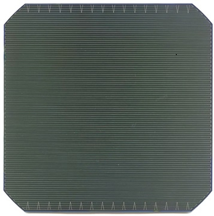
An international research group has fabricated a large-area bifacial TOPCon solar cell with passivating contacts based on in situ p-doped polycrystalline silicon (poly-Si) films, using low-pressure chemical vapor deposition (LPCVD).
The scientists adopted an industrial approach for LPCVD and used a homogeneous boron-diffused front emitter and screen-printed metallization. “The poly-Si film was deposited in … single-wafer LPCVD equipment,” the research corresponding author, Meriç Fırat, told pv magazine. “There are already tools available from tool manufacturers which are capable of LPCVD processes with in situ doping, with decent poly-Si film uniformity.”
The poly-Si films were integrated into the cell in two sets of experiments.
Through a first experiment, intended at assessing the impact of the films on cell performance, the researchers built a 241.3cm2 bifacial device with a zero-busbar design on both sides and a 70nm thick plasma-enhanced chemical vapor deposition (PECVD) hydrogenated silicon nitride (SiNx:H) film applied to the rear side for improving the passivation quality. “For metallization, silver and silver/aluminum pastes were screen-printed at the rear and front sides, respectively, followed by firing of the pastes through the SiNx:H films for realizing contacts with the poly-Si and the emitter,” they explained. “Firing was performed with a belt speed of 150in/min and a set peak temperature of 855 degrees Celsius.”
“The wraparound of the LPCVD poly-Si film at the front side was removed by masking the front side with a 200nm thick silicon monoxide (SiOx) mask grown by plasma-enhanced chemical vapor deposition … before LPCVD and using dry-etching,” Fırat stated. “We are confident that this part of the process can be simplified and transferred to industrial equipment capable of removing the unwanted poly-Si film at the front side by high-throughput single-side etching.”
Through a second experiment, aimed at investigating the impact of the rear surface morphology on the cell, the academics made the screening on a series of cells with a polished rear surface, a 90nm thick SiOx layer deposited by PECVD in a single-wafer system on top of the front SiNx:H film and a metal grid to create a double anti-reflection coating (DARC) intended at reducing front reflectance.
The performance of all solar cells was analyzed under standard illumination conditions and an inspection by optical microscopy was also conducted to assess the quality of the screen-printed contacts. The best performance was achieved by a cell with a polished rear surface using the DARC and consisting of a stack of 70nm SiNx and 90nm SiOx films. This device reached a power conversion efficiency of 23.01%, a high open-circuit voltage of 691.7 mV, a short-circuit current of 40.95 and a fill factor of 81.25%.
“The solar cells reported in our paper can be quite easily transferred to commercial production,” Fırat went on to say. “Some initial effort would be required to transfer the in situ doping-based LPCVD process to batch-type industrial equipment but we consider this to be achievable. The efficiency gain obtained with the DARC is probably not transferable to the module level, so I am still not sure if the DARC would be used in industrial production.”
The device was presented in the paper “Large-area bifacial n-TOPCon solar cells with in situ phosphorus-doped LPCVD poly-Si passivating contacts,” which was recently published in Solar Energy Materials and Solar Cells. The research group comprised scientists from Belgian research entities KU Leuven, VITO, imec and UHasselt, as well as from Kuwait University.
This content is protected by copyright and may not be reused. If you want to cooperate with us and would like to reuse some of our content, please contact: editors@pv-magazine.com.


1 comment
By submitting this form you agree to pv magazine using your data for the purposes of publishing your comment.
Your personal data will only be disclosed or otherwise transmitted to third parties for the purposes of spam filtering or if this is necessary for technical maintenance of the website. Any other transfer to third parties will not take place unless this is justified on the basis of applicable data protection regulations or if pv magazine is legally obliged to do so.
You may revoke this consent at any time with effect for the future, in which case your personal data will be deleted immediately. Otherwise, your data will be deleted if pv magazine has processed your request or the purpose of data storage is fulfilled.
Further information on data privacy can be found in our Data Protection Policy.