An international research group has developed a PV panel based on a cell technology featuring graphene-doped electron transporting layers (ETLs) and functionalized molybdenum disulfide (fMoS2) buffer layers inserted between the perovskite layer and the hole transporting layer (HTL).
“We have demonstrated that the use of two-dimensional materials such as graphene and MoS2 can be used to improve the performances of perovskite photovoltaic not only on lab devices but also in a real context with large area panels,” researcher Aldo di Carlo told pv magazine.
The scientists integrated the graphene flakes into the ETL to promote the crystallization of the perovskite wrapped within the ETL itself. They said this leads to a reduction in the electron trap density, while reducing the device's dark current and improving the cell's fill factor. Poly(triaryl)amine (PTAA), which is an excellent hole- transporting and electron-blocking material, was used for the HTL.
“At the perovskite–HTL interface, the buffer layer of fMoS2 flakes promotes the hole transfer from the absorbing layer to the HTL compared with reference devices without fMoS,” the researchers said. “In addition, the use of graphene and fMoS2 stabilizes the perovskite/ETL and perovskite/HTL interfaces, respectively, under harsh testing conditions, such as prolonged illumination and thermal stresses.”
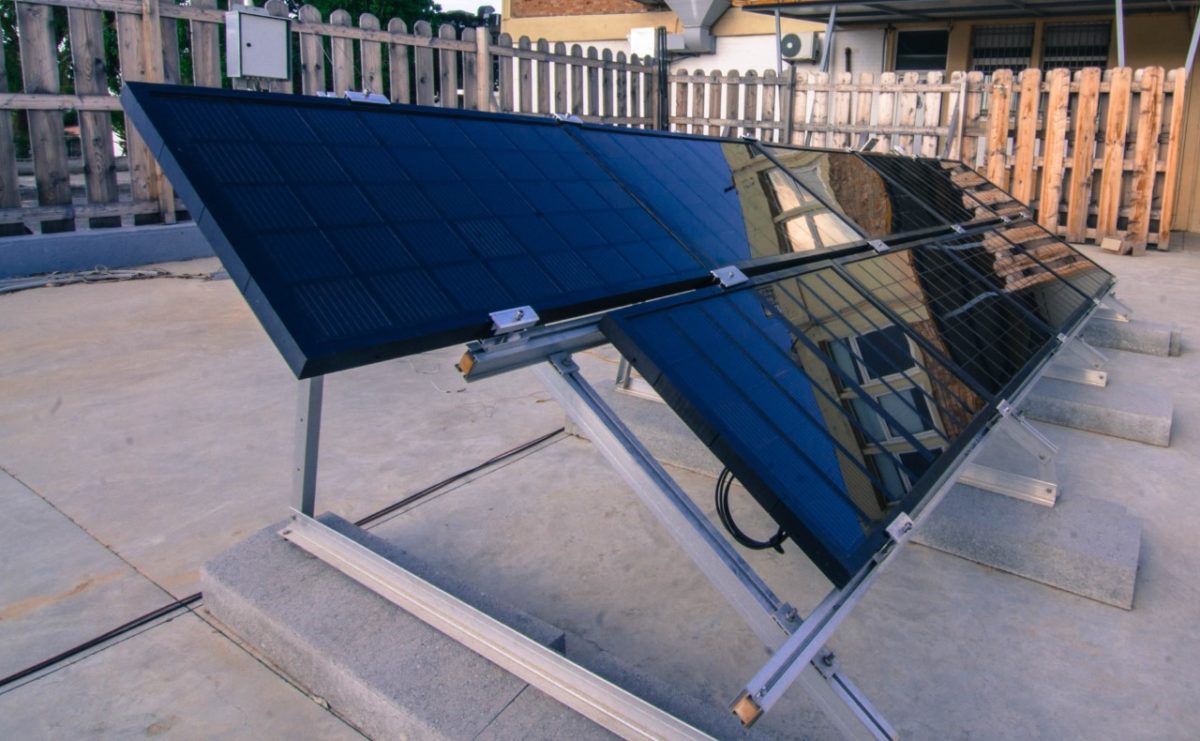
The module was fabricated with solar cells with an area of 9.1 cm2 and reached an active area of 81.9 square centimeters and an aperture area of 101 square centimeters. Its power conversion efficiency, measured under standard illumination conditions, is 12.5% and the fill factor reaches 81%.
“It is expected that the power conversion efficiency spread will be reduced by a fully automated perovskite solar module fabrication,” the researchers said.
The PV system is located at the campus of the Hellenic Mediterranean University (HMU) in Crete, Greece. The power generated by the facility is being stored in was stored in four serially connected 6 V vented tubular plate batteries with a capacity of 260 Ah. The modules have an area of 0.5 square meters and were used to build a standalone testing field with a total area of 4.5 square meters consisting of nine panels.
The group compared the performance of the panels with that of commercially available solar modules and found that the graphene-perovskite devices exhibited the smallest drop in open-circuit voltage with increasing temperature.
“The open-circuit voltage temperature coefficient of the graphene-perovskite panels is half of the one of crystalline silicon panels, simultaneously also exhibiting a larger positive short-circuit current temperature coefficient,” the scientists said. “At the same time, our results indicate that additional efforts are required to improve encapsulant materials and lamination protocol to extend further the panels’ lifetime.”
They introduced their findings in “Integration of two-dimensional materials-based perovskite solar panels into a stand-alone solar farm,” which was recently published in Nature Energy. The research group includes scientists from the University of Tor Vergata, the IIT Graphene Labs, the University of Siena, and GreatCell Solar Italia Srl in Italy, as well as Hellenic Mediterranean University in Greece.
“The data produced by the solar farm will be of fundamental importance for exploitation at the industrial level of the perovskite PV,” Di Carlo said.
This content is protected by copyright and may not be reused. If you want to cooperate with us and would like to reuse some of our content, please contact: editors@pv-magazine.com.


1 comment
By submitting this form you agree to pv magazine using your data for the purposes of publishing your comment.
Your personal data will only be disclosed or otherwise transmitted to third parties for the purposes of spam filtering or if this is necessary for technical maintenance of the website. Any other transfer to third parties will not take place unless this is justified on the basis of applicable data protection regulations or if pv magazine is legally obliged to do so.
You may revoke this consent at any time with effect for the future, in which case your personal data will be deleted immediately. Otherwise, your data will be deleted if pv magazine has processed your request or the purpose of data storage is fulfilled.
Further information on data privacy can be found in our Data Protection Policy.