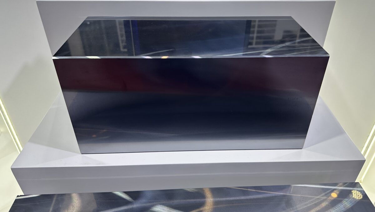
Researchers at Shandong University in China have investigated the fracture strength of commercial 210 mm x 210 mm monocrystalline silicon G12 wafers used for solar cell production and have found that several strategies may be adopted to produce large-size and ultra-thin silicon wafers while reducing fracture probability during the sawing process and the post-processing.
“We investigated the effect of wafer thickness on the fracture strength and the effect of the position of the silicon wafer in the silicon brick on the fracture strength of the silicon wafer,” the research's lead author, Yufei Gao, told pv magazine. “Four-point-bending (PB) tests were conducted on three thicknesses of G12 mono-Si wafers, and the load-displacement curves during the testing process were recorded.”
This kind of testing is used to assess the flexural strength of a material and its tendency to crack under the bending load. The material is usually placed on two supporting pins and centrally charged at two pressure lines with a testing piston.
For their analysis, the researchers used the finite element method (FEM), which is a numerical technique used to perform finite element analysis (FEA) of any given physical phenomenon, and the Weibull function, which is the most widely used in analyzing silicon wafer fracture.
“The basic assumption of the Weibull function is the weakest link assumption: the survival probability of a sample is the product of the survival probabilities of each volume element within the sample,” the scientists explained. “Therefore, the fracture strength of silicon wafers is determined by the weakest defect.”
They analyzed three different wafer thicknesses of 130 μm, 140 μm, and 150 μm and took into account the position of the silicon wafer in the silicon brick and the bending test direction.
The analysis showed that the surface roughness of the wafers decreases with the increase in the usage time of the saw wire. It also demonstrated that the curvature of the saw marks on the wafer surface grows with the increase of the usage time of the saw wire.
Furthermore, the team found that the distribution of the fracture probability density curve is more concentrated in the front wafers, while it is more dispersed in the rear wafers. It also ascertained that fracture characteristics of the middle wafers and the rear wafers are similar.
They also found that the characteristic fracture strength of bending in the perpendicular direction to the saw marks is two or three times that of bending in the parallel directions to the saw marks.
“The relationship between the saw wire usage time, the surface roughness, and the saw mark characteristics with silicon wafer fracture strength has been revealed, which provides the improvement direction for improving the strength of large-size ultra-thin silicon wafers and reducing the fracture probability in the production process,” the academics said.
This content is protected by copyright and may not be reused. If you want to cooperate with us and would like to reuse some of our content, please contact: editors@pv-magazine.com.


By submitting this form you agree to pv magazine using your data for the purposes of publishing your comment.
Your personal data will only be disclosed or otherwise transmitted to third parties for the purposes of spam filtering or if this is necessary for technical maintenance of the website. Any other transfer to third parties will not take place unless this is justified on the basis of applicable data protection regulations or if pv magazine is legally obliged to do so.
You may revoke this consent at any time with effect for the future, in which case your personal data will be deleted immediately. Otherwise, your data will be deleted if pv magazine has processed your request or the purpose of data storage is fulfilled.
Further information on data privacy can be found in our Data Protection Policy.