A Canadian research team has recently developed a micrometer-scale III-V solar cell for applications in concentrated photovoltaics (CPV).
Gallium arsenide (GaAs) and other III-V materials – named after the groups in the periodic table they belong to – are among the best known in terms of efficiency potential for solar cells. Their high production costs, however, have so far limited them to niche applications powering satellites and drones. In these devices, low weight and high efficiency are more pressing concerns than the cost of energy produced.
“The major drawback of these materials is their cost, typically more than two orders of magnitude more expensive than technology deployed on a large scale,” the scientists said. “To manage this problem, concentrated photovoltaic (CPV) technology promises to reduce costs by adding concentration optics to solar cells, thereby limiting the uses of III–V materials.”
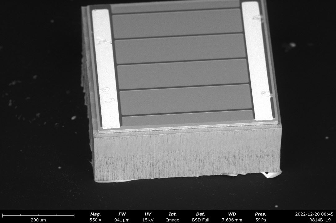
The proposed solar cell is based on indium gallium phosphide (InGaP), indium gallium arsenide (InGaAs) and germanium (Ge) and has an active area of 0.25 mm2.
“Our solar cell achieved the highest open-circuit voltage for InGaP/InGaAs/Ge of different size in the literature to our knowledge,” the research's lead author, Corentin Jouanneau, told pv magazine. “The device also achieved a power conversion efficiency of over 30%.”
In the paper “Fabrication and characterization of high performance sub-millimetric InGaP/InGaAs/Ge solar cells,” published in Solar Energy Materials and Solar Cells, Jouanneau and his team explained that they build the cell with a metal contact made of nickel (Ni) and gold (Au), as well as with an antireflective layer relying on silicon nitride (SiN) and silicon oxide (SiO).
The use of plasma process enabled wafer losses of less than 10% and the design of complex shapes, the team noted. They used a process based on plasma etching for cell isolation and singulation, which reportedly enables to manufacture solar cells of any size and shape. As a result, they were able to produce cells with a size ranging from 12.25 mm to 0.01 mm and different shapes: round, triangular, maple leaf, hexagonal.
The cells were then tested under standard illumination conditions, and a 0.25 mm2 cell was found to be the champion device with an efficiency of 30.61% and a record-breaking open-circuit voltage of 2.39 V. This result was attributed to “excellent” sidewall passivation.
The smallest device, measuring only 0.01 mm2, was found to reach an efficiency of 21.40%.
“These cells were not manufactured for their performance but to demonstrate the capabilities of plasma etching,” the academics explained, noting that their work was mainly intended to identify the cells that were most affected by perimeter recombinations.
This content is protected by copyright and may not be reused. If you want to cooperate with us and would like to reuse some of our content, please contact: editors@pv-magazine.com.


This micro III-V solar cell breakthrough is pretty exciting, especially with its crazy efficiency numbers and record-breaking open-circuit voltage. But I can’t help but have some mixed feelings about it.
Things That Make You Go “Hmm”
Is It Affordable? III-V materials are famously expensive. Even if they’re cutting costs by using concentration optics, it feels like we’re a long way from seeing this tech in everyday solar panels. Can they realistically make it cheap enough to compete with silicon-based options?
How Does It Handle the Real World? Sure, the lab results are impressive. But what happens when these tiny cells face real-life conditions—think temperature swings, rain, or partial shading? Lab efficiency is one thing; field performance is another.
Too Niche? These cells are tiny, and while that’s great for satellites or specialized tech, it doesn’t seem like they’ll make a big dent in the broader solar market any time soon.
The Bright Spots
Efficiency That’s Hard to Ignore: Over 30% efficiency and that record-setting voltage? That’s some next-level solar tech, even if it’s not ready for prime time.
Cool Custom Shapes: Making cells in all kinds of shapes—like a maple leaf—opens up creative possibilities for things like wearables, tech gadgets, or even solar art. It’s not just functional; it’s fun.
A Step Forward: Who knows? With more research and falling costs, this kind of tech might eventually make its way into our rooftops, delivering better bang for our buck.
The Big Question
Can this innovation move beyond niche uses and actually make a splash in the mainstream solar world? For now, it’s a promising glimpse into what’s possible, but it’s hard not to wonder if it’ll stay stuck as a high-tech novelty. Here’s hoping they can work out the kinks and make it something we can all use someday!