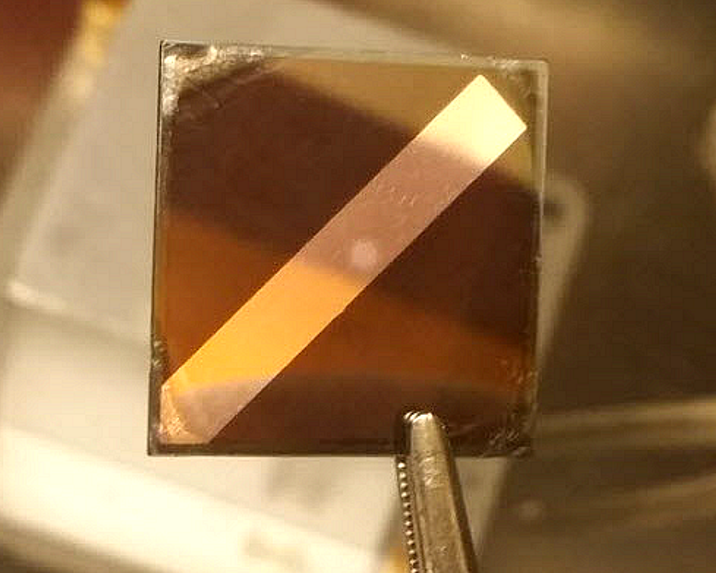
Scientists in Germany developed a technique using high precision photoluminescence to observe a perovskite solar cell; and detect where the material emits light in response to a laser light source. With this technique, the scientists were able to determine which areas and defects caused the biggest efficiency losses in the planar pin-type perovskite cells they worked with.
The results of the study ‘Visualization and suppression of interfacial recombination for high efficiency large-area pin perovskite solar cells’, published in the journal, Nature Energy, show that the interface between the perovskite absorber and the charge transport layers was responsible for a significant percentage of losses.
“This measurement method at our lab is so precise, we can determine the exact number of photons that have been emitted,” explains Thomas Unold, Deputy Head of HZB’s Structure and Dynamics of Energy Materials Department. “We were able to calculate the losses at every point of the cell and thereby determine that the most harmful defects are located at the interfaces between the perovskite absorber layer and the charge transport layers.”
Armed with this new information, the team was able to develop 1 cm² perovskite cells with 19.83% certified efficiency, stabilized power output, a high VOC (1.17 V) and record fill factor (>81%). This was achieved by inserting ultra thin layers between the two, leading to substantial loss reduction at both the p and n contacts.
The researchers also state that this method allowed them to produce cells with efficiencies higher than 20%, and that modified fabrication methods could provide another solution to the problem observed.
This content is protected by copyright and may not be reused. If you want to cooperate with us and would like to reuse some of our content, please contact: editors@pv-magazine.com.


By submitting this form you agree to pv magazine using your data for the purposes of publishing your comment.
Your personal data will only be disclosed or otherwise transmitted to third parties for the purposes of spam filtering or if this is necessary for technical maintenance of the website. Any other transfer to third parties will not take place unless this is justified on the basis of applicable data protection regulations or if pv magazine is legally obliged to do so.
You may revoke this consent at any time with effect for the future, in which case your personal data will be deleted immediately. Otherwise, your data will be deleted if pv magazine has processed your request or the purpose of data storage is fulfilled.
Further information on data privacy can be found in our Data Protection Policy.