Gallium arsenide (GaAs) and other III-V materials – named for their grouping in the periodic table – are well known as high performance solar cell materials, holding the majority of overall records for conversion efficiency.
But their high production costs, often in the range of hundreds of dollars per watt, have so far meant that such cells are limited to powering satellites, drones and other niche areas where cell performance takes precedence over cost-per-watt of generation capacity.
Bringing down these production costs to a level where mainstream solar applications can enjoy their performance potential is an important topic, and scientists in recent years have suggested a range of different approaches to this.
Growing the GaAs layers on a silicon substrate is one promising approach that would eliminate more expensive germanium from the mix, while allowing larger area fabrication. But layers produced in this way tend to have high levels of defects, limiting their performance in a solar cell.
Scientists led by the Université de Sherbrooke in Canada investigated whether using porous silicon, instead of crystalline silicon (c-Si), could lead to improvements. Results of their investigation are published in the journal Solar Energy Materials and Solar Cells, and show significant improvements in fill factor and open circuit voltage when substituting crystalline for porous silicon in an otherwise identical process.
Nanoheteroepitaxy
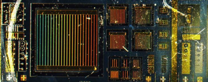
The group utilized a process called Nanoheteroepitaxy (NHE), where a semiconductor layer is grown on a patterned substrate. The group used a two-step growth process, first growing a GaAs buffer layer to close over the pores in the silicon, and then depositing the main film at a temperature of 565 degrees Celsius.
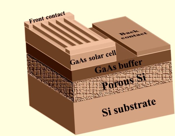
Image: Université de Sherbrooke
A cell measuring 1×1 mm, grown on porous silicon demonstrated a fill factor of 56%, compared with 41% for c-Si. The group put this down to fewer defects in the material, leading to lower recombination and parasitic losses.
The group notes that the level of defects in the cells it produced here would still need to be reduced to achieve worthwhile cell performance, and suggests that further experiments with increasing the porosity of the silicon to make it more flexible and better optimization of the buffer layer in the two-step growth process are worth investigating to achieve this.
This content is protected by copyright and may not be reused. If you want to cooperate with us and would like to reuse some of our content, please contact: editors@pv-magazine.com.


By submitting this form you agree to pv magazine using your data for the purposes of publishing your comment.
Your personal data will only be disclosed or otherwise transmitted to third parties for the purposes of spam filtering or if this is necessary for technical maintenance of the website. Any other transfer to third parties will not take place unless this is justified on the basis of applicable data protection regulations or if pv magazine is legally obliged to do so.
You may revoke this consent at any time with effect for the future, in which case your personal data will be deleted immediately. Otherwise, your data will be deleted if pv magazine has processed your request or the purpose of data storage is fulfilled.
Further information on data privacy can be found in our Data Protection Policy.