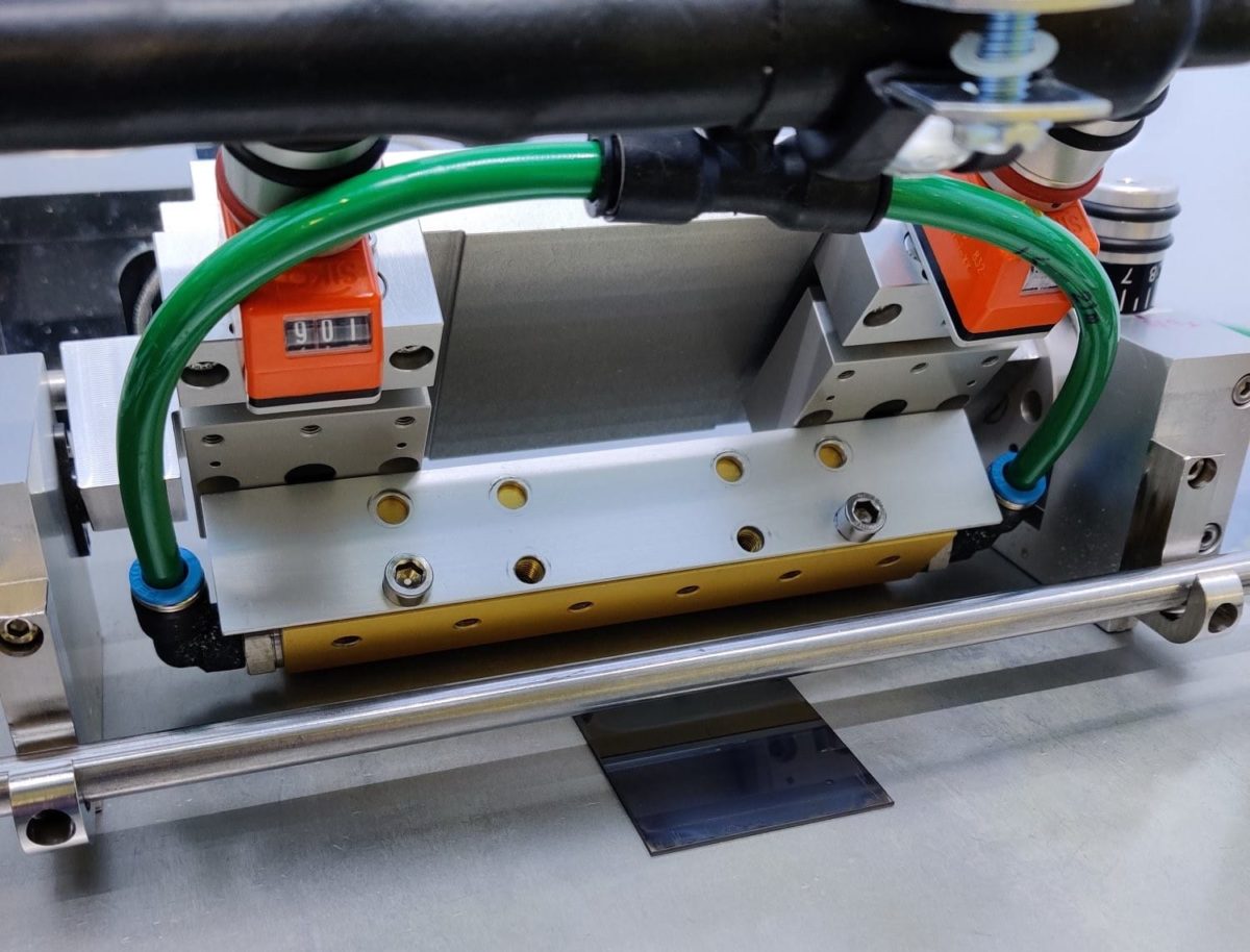
Researchers at France's National Solar Energy Institute (INES) – an arm of the French Alternative Energies and Atomic Energy Commission (CEA) – have fabricated an 18%-efficient mini perovskite solar module with a surface of 10 cm².
The panel was developed with a special perovskite material that is also known as CsxFA1-xPb(I1-yBry)3). The material has no methylammonium and includes multiple types of cations and a mix of halogens.
The manufacturing process, according to the researchers, is easy to scale up, as it combines a coating step carried out in air followed by a gas quenching conversion step to form the desired perovskite material.
The perovskite layer is formed at a low temperature of less than 100 Celsius degrees and is then integrated into the modules using laser ablation as a structuring process, thus minimizing inactive areas. The device's fill factor is over 93%. The time required for the deposition of the perovskite layer on an M2 wafer is estimated to be around 30 seconds, which is by far the fastest process for large-scale, high-volume production, according to the scientists.
Popular content
The proposed manufacturing technique is also claimed to be compatible with the integration of perovskite into heterojunction silicon solar cells in tandem architecture. Enel Green Power, the renewables unit of Italian utility Enel, and CEA-INES announced in August an efficiency of 25.0% for a heterojunction solar cell with an active surface of 213 cm2, based on the M2 silicon wafer format.
This content is protected by copyright and may not be reused. If you want to cooperate with us and would like to reuse some of our content, please contact: editors@pv-magazine.com.


By submitting this form you agree to pv magazine using your data for the purposes of publishing your comment.
Your personal data will only be disclosed or otherwise transmitted to third parties for the purposes of spam filtering or if this is necessary for technical maintenance of the website. Any other transfer to third parties will not take place unless this is justified on the basis of applicable data protection regulations or if pv magazine is legally obliged to do so.
You may revoke this consent at any time with effect for the future, in which case your personal data will be deleted immediately. Otherwise, your data will be deleted if pv magazine has processed your request or the purpose of data storage is fulfilled.
Further information on data privacy can be found in our Data Protection Policy.