A group of scientists from Australia has investigated how consumer flatbed scanners may be used to monitor the optical properties of solar cells and have found that these devices may offer results comparable to those of high-end tools used in the photovoltaic industry for some types of cells and wafers.
“Flatbed office scanners are widely available, have typical costs in the hundreds of dollars, provide high spatial resolution, and include a built-in white light source enabling measurements across three different colors channels,” said researchers from Macquarie University and the University of New South Wales (UNSW). “Office scanners have found similar unintended uses for monitoring radiation, a range of biomedical imaging applications and for monitoring components’ physical dimensions.”
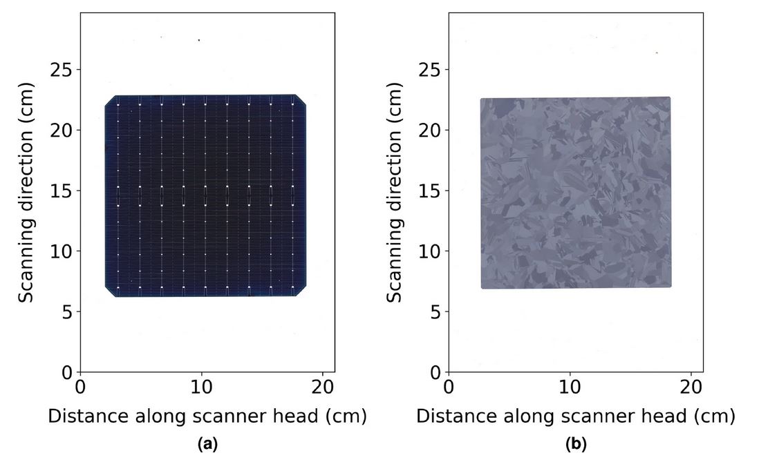
In their experiment, the researchers used a Contact Image Sensor (CIS) scanner, which works by being almost in direct contact with the object to be scanned, to monitor the spatial variation in the texture of multi-crystalline and mono-crystalline wafers prepared with varying texture conditions. Its performance was compared to that of the Loana system which is commonly utilized in the solar industry and at the research level.
The academics took measurements of several wafers with varying textures via the CIS scanner and compared them to reflection maps performed with a Loana system. “A good correlation was observed for all metrics for the multi-crystalline wafers of varying textures,” they emphasized. “This is true both when comparing between samples and when comparing spatial data across a single multi-crystalline sample.”
According to them, these results confirm that the low-cost scanner technology is suitable for monitoring polycrystalline devices, although they do not extend to monocrystalline wafers. “The reflection of the random pyramid texture caused by the alkaline texturing process is not well captured by the scanner. This is believed to occur as a result of the different physical mechanisms of texture formation and how those textures scatter light,” they also stated, referring to the monitoring of the monocrystalline devices.
“Both good qualitative agreement and statistical correlation were achieved between the scanner and industry tool for the isotropic multi-crystalline wafers,” they concluded.
They presented their findings in the paper “Determining the optical properties of solar cells using low cost scanners,” published in Scientific Reports. The research group comprised four scientists from Macquarie University and UNSW.
This content is protected by copyright and may not be reused. If you want to cooperate with us and would like to reuse some of our content, please contact: editors@pv-magazine.com.


1 comment
By submitting this form you agree to pv magazine using your data for the purposes of publishing your comment.
Your personal data will only be disclosed or otherwise transmitted to third parties for the purposes of spam filtering or if this is necessary for technical maintenance of the website. Any other transfer to third parties will not take place unless this is justified on the basis of applicable data protection regulations or if pv magazine is legally obliged to do so.
You may revoke this consent at any time with effect for the future, in which case your personal data will be deleted immediately. Otherwise, your data will be deleted if pv magazine has processed your request or the purpose of data storage is fulfilled.
Further information on data privacy can be found in our Data Protection Policy.