Researchers from the National University of Singapore have fabricated an ultra-thin TOPCon solar cell with polysilicon (poly-Si) passivated contacts on both sides – a so-called byPoly solar cell – using low-pressure chemical vapor deposition (LPCVD).
Poly-Si layers are used in TOPCon devices to improve passivation and carrier transport. In these structures, a thin interfacial oxide reduces surface recombination by electrically and chemically passivating the silicon interface, while the overlying doped polycrystalline silicon layer provides a low-resistance pathway for majority carriers.
“Due to its simple structure and good low‑light performance, the cell is suitable for building-integrated photovoltaics (BIPV), indoor low‑light energy harvesting, wearable electronics, portable power supplies and solar quadcopters,” research lead author Aaron Danner told pv magazine.
“The proposed selective bipoly solar cell is currently in the lab‑scale research stage and is not yet ready for commercial production,” he went on to say. “Further work on large‑area fabrication, manufacturing‑line compatibility, long‑term stability validation and flexible packaging optimization is essential for future industrial deployment.”
In the study “Ultra-Thin Bipoly Solar Cells With Front Selective n-Type TOPCon and Rear Blanket p-Type TOPCon Layers,” published in Progress in Photovoltaics, the research team explained that byPoly solar cells, which are often referred to as double-sided TOPCon, offer substantial improvements in both surface passivation and charge carrier transport, by virtue of careful optimization of the doping levels and interfacial properties of the two poly-Si layers, which effectively suppresses recombination losses while preserving a high open-circuit voltage and fill factor.
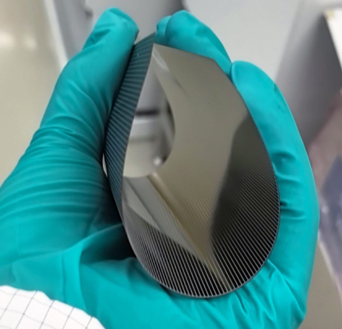
The solar cells were fabricated using M2-sized Czochralski silicon wafers, which were thinned from 180 μm to 80 μm via a stress-driven etching (SDE) process. Standard Radio Corporation of America (RCA) cleaning was performed to remove organic, metallic, and particulate contaminants prior to processing.
A brief hydrofluoric acid (HF) dip removed native oxides, followed by rear-side protection with plasma-enhanced chemical vapor deposition (PECVD) silicon nitride (SiNx) and front-side potassium hydroxide (KOH) texturing, which simultaneously eliminated unwanted polycrystalline silicon and formed pyramidal light-trapping structures.
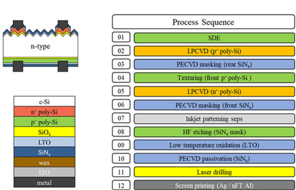
Image: National University of Singapore, Progress in Photovoltaics, CC BY 4.0
A full-area doped poly-Si layer was then deposited on both sides via low-pressure chemical vapor deposition (LPCVD), followed by HF treatment to remove native oxide. Selective patterning retained poly-Si only beneath metal contacts, minimizing optical losses while preserving carrier transport, after which the SiNx mask was removed and the surfaces re-cleaned for passivation.
A thin low-temperature oxide (LTO) layer was grown to improve interface quality, followed by PECVD SiNx deposition as both passivation and anti-reflection coating. Rear-side contacts were opened using laser contact opening (LCO), enabling screen-printed aluminum (Al) metallization, while front-side silver (Ag) contacts were printed over the selective poly-Si regions. Final co-firing at 740 C completed device fabrication.
Using quasi-steady-state photoconductance (QSSPC) and photoluminescence (PL) measurements, the scientists found that the champion device built with the proposed architecture, with thickness of of 80 μm, achieved a power conversion efficiency of 19.7%, corresponding to an efficiency-to-thickness ratio of 0.25% per μm. The cell also reached an open-circuit voltage of up to 719 mV and a fill factor exceeding 83%.
“The favorable device performance is attributed to the optimized thermal treatment of the poly-Si layers, which enhances dopant activation and interface quality, thereby reducing recombination losses,” the researchers said, noting that the ultra-thin cells also exhibited noticeable mechanical flexibility, which enables potential use in curved or non-planar applications such as aerospace and wearable systems.
“Although quantitative cost analysis is not fully performed in this fundamental study, the proposed cell adopts fully silicon‑compatible fabrication processes with no additional high‑cost materials or complex procedures,” Danner explained. “Its manufacturing cost is almost comparable to conventional silicon‑based solar cells, demonstrating outstanding low‑cost industrialization potential for mass production.”
“With our work, we presented a quantitative evaluation of the interplay between surface passivation quality, optical engineering, and mechanical stability in ultra-thin silicon solar cells. Although the results demonstrate the feasibility of biPoly-based device architectures, further optimization is needed in areas such as contact resistivity, thermal stability, and long-term reliability under cyclic mechanical deformation,” he concluded.
This content is protected by copyright and may not be reused. If you want to cooperate with us and would like to reuse some of our content, please contact: editors@pv-magazine.com.


By submitting this form you agree to pv magazine using your data for the purposes of publishing your comment.
Your personal data will only be disclosed or otherwise transmitted to third parties for the purposes of spam filtering or if this is necessary for technical maintenance of the website. Any other transfer to third parties will not take place unless this is justified on the basis of applicable data protection regulations or if pv magazine is legally obliged to do so.
You may revoke this consent at any time with effect for the future, in which case your personal data will be deleted immediately. Otherwise, your data will be deleted if pv magazine has processed your request or the purpose of data storage is fulfilled.
Further information on data privacy can be found in our Data Protection Policy.