Researchers from Australian National University and Chinese PV module manufacturer Longi investigated the wafer quality of n-type industrial ingots made via the Recharged Czochralski (RCz) process, applying two defect mitigation strategies – Tabula Rasa (TR) and phosphorus diffusion gettering (PDG) – to further improve the bulk lifetimes.
TR is commonly used to dissolve any oxygen clusters or precipitates in Cz ingots, while the PDG involves three steps and is utilized during crystal growth to remove containments and other forms of defects in wafers. Through gettering, the impurities are initially released into a solid solution and then undergo diffusion through the silicon. Finally, they are trapped in an area away from the active circuit regions of the wafer.
“The most surprising finding was the extent to which melt recharging can consistently produce very high quality material, which has positive implications for improving solar cell efficiencies,” corresponding author, Afsaneh Kashizadeh, told pv magazine. “The most challenging aspect of the study was accurately measuring Auger-limited lifetimes using research lab equipment. This required meticulous calibration and repeated validation of our surface passivation films and measurement techniques.”
The implementation of the two strategies was followed by a high-temperature boron diffusion step, which the research team said was representative of the highest thermal budget step in the tunnel oxide passivated contact (TOPCon) cell fabrication process.
The Recharged Czochralski (RCz) crystal growth process, which enables crucible re-use without powering down between pulls, is increasingly used to produce ingots for both n-type and p-type wafers due to its productivity and cost-reducing benefits.
To investigate the quality of RCz n-type wafers, the researchers first characterized the as-grown material before subjecting the test material to high-temperature processes. The samples were measured directly on the ingots and passivated wafers.
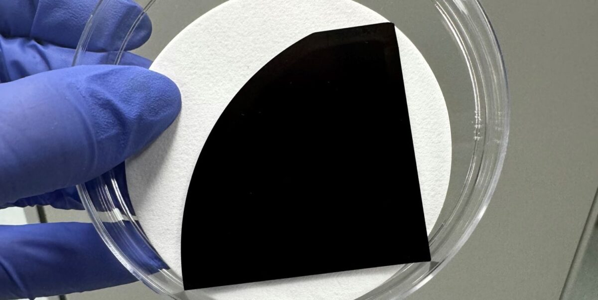
The group grew seven ingots with a single crucible and then selected three ingots to create wafers cut from 16 different positions from each of the three ingots, noting that these had different solidified fractions. Wafers supplied by Longi were laser-cut from the center of pseudo-square M10-sized n-type RCz silicon wafers.
There were three specimen groups, one that remained untreated, a second group that underwent the TR treatment in a conventional quartz tube furnace for 30 minutes in an oxygen environment, and the third group was PDG treated.
“Our study reveals that industrial n-type wafers grown via RCz are close to the Auger limit under open-circuit conditions in the as-cut state, and that after PDG they effectively reach this limit,” stated the team. “Our results show that implied maximum power point voltage improved by 5-15 mV, particularly near the tail-end, suggesting that these wafers will benefit from the gettering process provided by standard TOPCon processes, although these may be somewhat different to those employed in this study, or from a pre-gettering step for heterojunction cells.”
The researchers also noted that the wafers will “benefit from the gettering process provided by standard TOPCon processes, although these may be somewhat different to those employed in this study, or from a pre-gettering step for heterojunction cells.”
They also found that, after boron diffusion, the bulk lifetimes of the samples did not decrease considerably, which suggests these wafers are resilient to high thermal budgets. “We also conclude that the quality of subsequently-grown ingots does not decrease significantly, even after multiple ingots are pulled from the recharged melt, and whole ingots can be suitable for high-efficiency solar cells without any need for further high-temperature processes,” they said
The details of the experiment, including wafering, etching and cleaning steps, tests, and results were described in “Auger-limited Bulk Lifetimes in Industrial Czochralski-Grown n-Type Silicon Ingots with Melt Recharging,” published in Solar Energy Materials and Solar Cells.
According to Kashizadeh, the interest of peers in the study has centered on the notable “ability to control oxygen concentration at low levels and achieving high lifetimes throughout the process without relying on methods such as magnetic confinement of the melt.
Looking ahead, she noted plans to investigate the quality of next-generation n-type silicon wafers doped with antimony. “Preliminary results indicate that these wafers have higher mechanical strength compared to phosphorus-doped ones. Additionally, we are observing more uniform resistivity throughout the ingot growth process,” said Kashizadeh.
This content is protected by copyright and may not be reused. If you want to cooperate with us and would like to reuse some of our content, please contact: editors@pv-magazine.com.


By submitting this form you agree to pv magazine using your data for the purposes of publishing your comment.
Your personal data will only be disclosed or otherwise transmitted to third parties for the purposes of spam filtering or if this is necessary for technical maintenance of the website. Any other transfer to third parties will not take place unless this is justified on the basis of applicable data protection regulations or if pv magazine is legally obliged to do so.
You may revoke this consent at any time with effect for the future, in which case your personal data will be deleted immediately. Otherwise, your data will be deleted if pv magazine has processed your request or the purpose of data storage is fulfilled.
Further information on data privacy can be found in our Data Protection Policy.