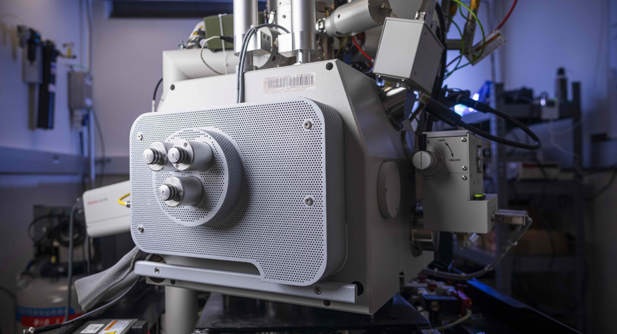
Researchers from the University of California Santa Barbara have visualized photoexcited charges traveling across the interface of two different semiconductor materials within a solar cell.
In a solar cell, sunlight hits a semiconductor material causing electrons to move across two different materials, known as the heterojunction, creating a current that is harnessed to power electronic devices. It is understood that this research is the first time this movement of photocarriers, which lasts picoseconds, or trillionths of a second, has been captured as a moving visual.
The research paper, “Imaging hot photocarrier transfer across a semiconductor heterojunction with ultrafast electron microscopy,” available in the journal PNAS, details how the researchers used ultrafast electron microscopy (SUEM), a technique combining high spatial-temporal resolution and surface sensitivity, to investigate photocarrier dynamics across a silicon and germanium heterojunction, both common semiconductor materials in photovoltaics.
The team used ultrafast laser pulses to act as a picosecond-scale shutter and fired an electron beam to scan the surface of the materials through which the hot photocarriers travel, excited by an optical pump beam. The resulting images allowed the team to assess the photocarriers as they diffuse from one semiconductor material to the other.
In the research paper, the researchers discuss how the heterojunction drastically modifies the hot photocarrier diffusivities in both silicon and germanium regions due to charge trapping, resulting in reduced carrier mobility. They say this can negatively affect the performance of devices that separate and collect these hot charges.
“If you excite charges in the uniform silicon or germanium regions, the hot carriers move very, very fast; they have a very high speed initially because of their high temperature,” explained Bolin Liao, an associate professor of mechanical engineering and one of the researchers. “But if you excite a charge near the junction, a fraction of the carriers are actually trapped by the junction potential, which slows them down.”
Liao added that while the charge trapping in silicon/germanium heterojunctions can be understood by semiconductor theory, it was still striking to directly observe it experimentally.
“We didn’t expect to be able to image this effect directly,” he said, suggesting semiconductor device designers may want to address the phenomenon. “This paper is really about demonstrating the capability of SUEM to, for example, study realistic devices.”
This content is protected by copyright and may not be reused. If you want to cooperate with us and would like to reuse some of our content, please contact: editors@pv-magazine.com.


By submitting this form you agree to pv magazine using your data for the purposes of publishing your comment.
Your personal data will only be disclosed or otherwise transmitted to third parties for the purposes of spam filtering or if this is necessary for technical maintenance of the website. Any other transfer to third parties will not take place unless this is justified on the basis of applicable data protection regulations or if pv magazine is legally obliged to do so.
You may revoke this consent at any time with effect for the future, in which case your personal data will be deleted immediately. Otherwise, your data will be deleted if pv magazine has processed your request or the purpose of data storage is fulfilled.
Further information on data privacy can be found in our Data Protection Policy.