Chinese startup claims record-breaking 27.87% efficiency for single-junction perovskite solar cell
Shenzhen-based SolaEon has reported a 27.87% efficiency for a single-junction perovskite solar cell on a 0.076 cm² lab device, certified by China’s National Photovoltaic Industry Metrology and Testing Center.
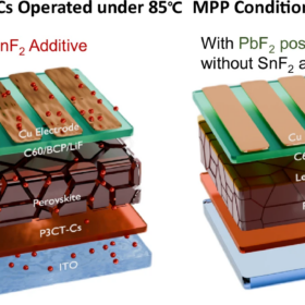
Scientists build tin lead perovskite solar cell with 24.07% efficiency
A Chinese-Swedish research team has boosted the performance of tin-lead perovskite solar cells by modifying additives and post-treatment processes. The device also demonstrated improved stability, retaining 60% of its initial efficiency after 550 hours at 85 °C under maximum power point conditions.

Australian startup moves forward with perovskite solar manufacturing plans
Halocell Energy is set to benefit from the development of a sovereign supply chain for high-purity precursors to perovskite after signing a memorandum of understanding with Queensland advanced materials company Lava Blue.

Scientists achieve 32.6% efficiency in perovskite-silicon tandem solar cell via interface engineering
Researchers from KAUST, TU Delft, and LMU Munich have improved the performance of monolithic perovskite-silicon tandem solar cells by modifying the physical structure at the front of the bottom heterojunction solar cell.

Scientists achieve 25.4% efficiency in perovskite solar cells with enhanced stability using multivalent ligands
Researchers have used multivalent amidinium ligands to boost perovskite solar cell efficiency to 25.4%, achieving over 95% stability after 1,100 hours at 85 C. The proposed approach enables controlled low-dimensional passivation layers, offering a practical route for durable, large-area perovskite devices.
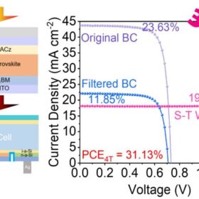
Chinese scientists build 31.13%-efficient perovskite-silicon tandem solar cell via 2D seeding agent
Researchers in China developed a novel two dimensional (2D) seeding agent to regulate crystallization in a 1.80-eV wide-bandgap perovskite film. A perovskite-silicon tandem device made with the resulting optimized subcell achieved an efficiency of 31.13%, outperforming a control device.
Researchers achieve record perovskite solar module stability under light, heat, and UV stress
An international research team has developed a new two-dimensional perovskite interlayer based on a co-crystal engineering strategy for more robust perovskite films. It demonstrated improved performance in small area perovskite solar cells and, in a 48 cm2 module, contributed to retain 95% of initial efficiency after 5,000 h.
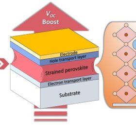
EPFL researchers enhance perovskite solar cell performance via rubidium
Researchers led by Michael Grätzel at the Ecole Polytechnique Federale de Lausanne in Switzerland have recently led efforts to improve perovskite optoelectronic properties using small-radius rubidium ion chemistry to enable more stable and efficient perovskite solar cells.
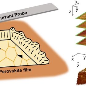
New research sheds light on defect regions in perovskite solar films
A Chinese research group has demonstrated an electrical imaging technique using 3D tomographic conductive atomic force microscopy to investigate passivation strategies of perovskite films to improve stability and efficiency of perovskite solar cells.

Leecell develops organic PV for indoor, outdoor use
The South Korean startup is developing organic solar cell technology made using a proprietary roll-to-roll process. It targets both indoor and outdoor integrated PV applications.
