In recent months, the rapidly shrinking price gap between monocrystalline and multicrystalline solar modules has created widespread expectation in the PV industry that monocrystalline technology will take the lead over its multicrystalline counterpart.
Analysts predict that the market share of monocrystalline cells and modules will rapidly increase from 33% in 2017, to 70% or even higher, within just a few years.
One argument that many observers quote is that monocrystalline wafers offer a larger potential for high-efficiency cells than multicrystalline wafers do.
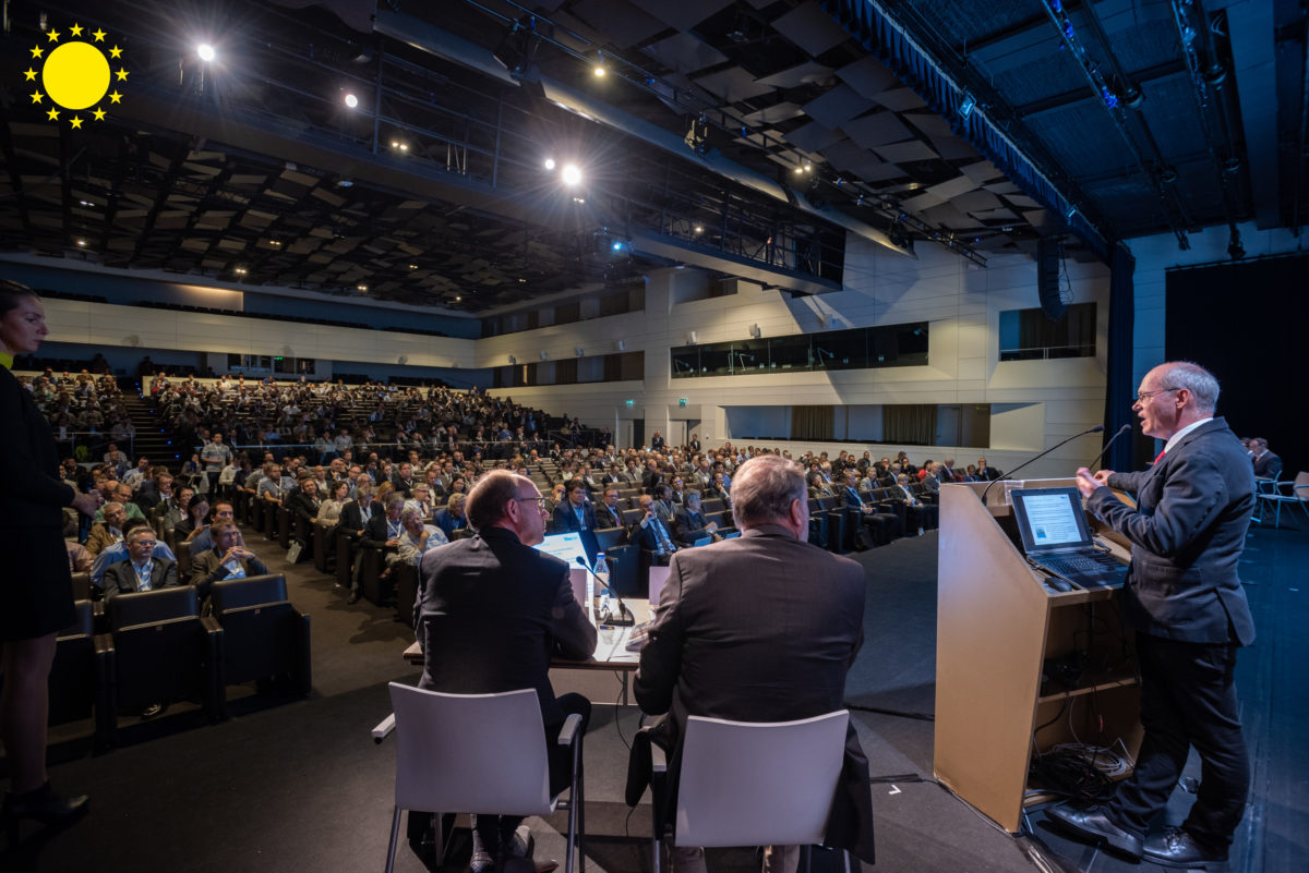
At the 35th European Photovoltaic Solar Energy Conference (EU PVSEC) held in Brussels this week, the mono advocates were able to find further evidence for their case, as the conference traditionally features a lot of monocrystalline high-efficiency concepts.
Record efficiency of 26.1% for back-contact lab cell
One of the student award winners, Christina Klamt from the Institute for Solar Energy Research Hamelin (ISFH/Germany), for instance, presented a record efficiency of 26.1% for a 4 cm² small, monocrystalline laboratory cell made of high-quality float-zone silicon with an interdigitated back-contact (IBC) structure, where both positive and negative contacts are positioned on the rear side of the positively doped (p-type) cell, thus avoiding any shading on the front side.
Moreover, the cell uses passivating contacts, which have become a new research direction since 2013. Such contacts are built by covering the rear side of the silicon wafer with a very thin dielectric layer of silicon oxide, which passivates the boundary, followed by a p- or n-doped polycrystalline silicon film and a metallization layer.
Depending on the dopant, only electrons or only holes are able to either tunnel directly through the thin silicon oxide or to migrate through pin holes in it, in order to get to the metal contact.
With such a selective passivating contact on the full rear side of an n-type lab cell, the Fraunhofer Institute for Solar Energy Systems has also achieved a record efficiency of 25.8%, although it still uses a conventional metal contact on the front side.
Industrial monocrystalline cells approaching 23% and more
Monocrystalline cell concepts that are closer to today’s industrial production processes were also presented at the EU PVSEC, but even those yielded remarkable results.
In cooperation with the École Polytechnique Fédérale de Lausanne (EPFL) and the Centre Suisse d'Electronique et de Microtechnique (CSEM), the research unit of Swiss equipment manufacturer, Meyer Burger has developed a heterojunction cell with an interdigitated back contact.
Using a shadow mask for building the contact fingers on the rear side, the production of the cell requires only 10 process steps. Meyer Burger has thus achieved an efficiency of 23.8% on a cell area of 90.25 cm².
For industrial monocrystalline p-type cells, the Passivated Emitter and Rear Cell (PERC) has already become mainstream.
A variant for n-type wafers is PERT (Passivated Emitter Rear Totally diffused), where the emitter is shifted from the front to the rear side of the cell. Applying the PERT structure to an industrial-size 6-inch wafer, the Interuniversity Microelectronics Centre (Imec) in Leuven (Belgium) has achieved an efficiency of 23.0%.
But even with the standard PERC concept, similar efficiencies are within reach. Hanwha Q-Cells is already producing monocrystalline PERC cells (the company calls them “PERC-like”), with an average efficiency of 22.15% and a peak value of 22.4%.
At the EU PVSEC, research and development engineer, Benjamin Lee presented the next step: By introducing a selective emitter on the front side, the peak efficiency increases to 22.7%.
A new concept for the cell front side
One reason why p-type PERC has made its breakthrough in the industry is the exponential cost decline for the necessary manufacturing equipment.
Pietro Altermatt, Principal Scientist at Trina Solar, highlighted this success story and made a case for keeping the PERC structure on the rear side of the cell; the industry should focus on the cell front side as this would offer more room for improvements.
The scientist proposed to cover the front side with a thin silicon oxide layer and an n-doped transparent oxide, such as aluminium-doped zinc oxide, on top, which is then contacted by metal fingers.
This transparent hetero-emitter with a passivating contact causes the electrons in the silicon bulk to move laterally underneath the silicon oxide layer, and to tunnel through it in the region of the metal fingers.
Via this trick, the transparent oxide does not need to conduct the electrons laterally towards the contact fingers. Silicon nitride on top is used as an anti-reflection coating.
Whichever solution for the front side will prevail, Altermatt predicted that the average efficiency of industrial PERC cells will approach 24% by 2025.
Multicrystalline technology is keeping abreast
In view of such bright perspectives for monocrystalline technology, do multicrystalline solar cells still have any chance on the market at all?
Hanwha Q-Cells is a good addressee for this question: Although it is one of the efficiency leaders for monocrystalline PERC, the company still maintains 50% of its production capacity for multicrystalline modules.
“The prospects for multi are still quite good. There is still a reasonable future for that technology,” Q-Cells engineer, Lee said at the conference.
Chinese cell producer GCL System Integration Technology (GCL-SI) has demonstrated why. The company has improved the peak efficiency of its multicrystalline PERC cells with a black-silicon texture on diamond-wire-sawn wafers, from 20.8% presented at last year’s EU PVSEC, to 21.6% now.
Compared with the peak efficiency of 22.4% for the mono PERC cell (without selective emitter) from Hanwha Q-Cells, this is a difference of 0.8% absolute.
Peter Fath, CEO of the German equipment supplier, RCT Solutions and chairman of the session featuring GCL-SI’s presentation, argues that multicrystalline cells will remain competitive as long as their efficiencies are in a distance of 1.0% to 1.2% to monocrystalline cells.
GCL-SI is using reactive ion etching (RIE) for creating the black-silicon texture. While this method delivers the highest cell efficiencies, it is relatively expensive.
Fath believes that combining less expensive metal-catalyzed chemical etching (MCCE) for the main job and RIE for the finishing part will be a cost-effective solution. His conclusion was unshaken by the current mono hype: “Multicrystalline silicon will not die.”
By Johannes Bernreuter
This content is protected by copyright and may not be reused. If you want to cooperate with us and would like to reuse some of our content, please contact: editors@pv-magazine.com.


2 comments
By submitting this form you agree to pv magazine using your data for the purposes of publishing your comment.
Your personal data will only be disclosed or otherwise transmitted to third parties for the purposes of spam filtering or if this is necessary for technical maintenance of the website. Any other transfer to third parties will not take place unless this is justified on the basis of applicable data protection regulations or if pv magazine is legally obliged to do so.
You may revoke this consent at any time with effect for the future, in which case your personal data will be deleted immediately. Otherwise, your data will be deleted if pv magazine has processed your request or the purpose of data storage is fulfilled.
Further information on data privacy can be found in our Data Protection Policy.