Scientists at Massachusetts Institute of Technology (MIT) and the U.S. National Renewable Energy Laboratory (NREL) have outlined the case for reducing the thickness of solar wafers from the current industry standard of 160 microns down to 50 microns and even thinner, arguing that the potential cost benefits of such a move are too big to ignore and that technologies exist to overcome the challenges inherent to producing and handling such thin materials.
Reducing silicon consumption by moving to thinner wafers is not a new idea. The introduction of diamond wire sawing around 2016 brought about major cost reductions, thanks in part to reducing silicon consumption. But falling prices for silicon made this less of a priority, and the industry has since focused on alternative routes to cost reduction.
According to this latest analysis from MIT and NREL, however, many of these alternative routes have now been exhausted, and the industry could once again benefit from returning its focus to wafers – still the most expensive component in a module. “Efficiency can only go up by a few percent. So if you want to get further improvements, thickness is the way to go,” explains Tonio Buonassisi of MIT’S Photovoltaic Research Laboratory. “There is a path. It’s not easy, but there is a path. And for the first movers, the advantage is significant.”
The full analysis is available in the paper Revisiting thin silicon for photovoltaics: a technoeconomic perspective, published in the journal Energy & Environmental Science. The researchers suggest that thinner wafers could greatly reduce costs by producing more wafers per silicon ingot, increasing production capacity without the need to build capital intensive new factories.
The challenge in reducing wafer thickness beyond the current standard of 160 microns is that the material becomes brittle, leading to more microcracks and higher breakage rates in production. MIT postdoc Zhe Liu estimates that with current technology it should be “relatively simple” to go down to 100 microns, and in the future new innovations could make wafers as thin as 15 microns viable.
“This area is ripe for innovation, a sentiment echoed by forward-looking industry players,” concludes the research paper. “Now, the main barrier that hinders the widespread adoption of thin wafers is likely to be manufacturing yield loss. We believe the industry is ready for thin wafers, but an extra effort on developing innovative manufacturing equipment and processes is necessary to overcome this barrier.”
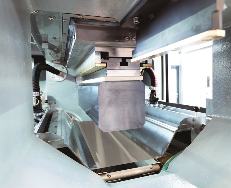
U.S. based startup 1366 Technologies has suggested one solution to this, with its ‘Direct Wafer Process’, where wafers are produced directly from molten silicon rather than cut from a larger ingot. This allows the wafer to be produced slightly thicker at certain points, reducing its brittleness.
But MIT suggests that even broader action may be needed to facilitate such a change. “What may be required is for the different key players in the industry to get together and lay out a specific set of steps forward and agreed upon standards,” says Buonassisi. “That would be truly transformative.”
This content is protected by copyright and may not be reused. If you want to cooperate with us and would like to reuse some of our content, please contact: editors@pv-magazine.com.


3 comments
By submitting this form you agree to pv magazine using your data for the purposes of publishing your comment.
Your personal data will only be disclosed or otherwise transmitted to third parties for the purposes of spam filtering or if this is necessary for technical maintenance of the website. Any other transfer to third parties will not take place unless this is justified on the basis of applicable data protection regulations or if pv magazine is legally obliged to do so.
You may revoke this consent at any time with effect for the future, in which case your personal data will be deleted immediately. Otherwise, your data will be deleted if pv magazine has processed your request or the purpose of data storage is fulfilled.
Further information on data privacy can be found in our Data Protection Policy.