Silver bismuth sulfide (AgBiS2) nanocrystals (NCs) are an earth-abundant material that has been used in recent years as a promising PV material, often in combination with cadmium sulfide in the development of several kinds of ultra-thin solar cells.
Solar cells built with these nanocrystals have so far reached efficiencies of up to 9% and their optoelectronic overall properties have been found to change drastically as their composition and size are changed. Their fabrication can be performed in air at low temperatures using low-cost solution processing techniques and inexpensive production equipment. Furthermore, AgBiS2 NCs have very low toxicity compared to other materials used for thin-film solar cells, such as cadmium telluride and cadmium sulfide.
With this in mind, researchers at the Institute of Photonic Sciences (ICFO) in Spain have fabricated an AgBiS2 PV device that exceeded the 10% efficiency threshold for the first time.
“AgBiS2 has recently emerged as a promising ternary semiconductor that is free of toxic heavy metals and has been shown to possess extraordinary optical properties including the highest optical absorption amongst any other photovoltaic absorber,” the research's lead author, Gerasimos Konstantatos, told pv magazine. “That resulted in a power conversion efficiency of over 9%, which was achieved using a layer-by-layer solid-state ligand exchange process that, however, is not suitable for large-area high-volume manufacturing needed for PV deployment.”
The 9% efficiency threshold refers to a 9.7%-efficient AgBiS2 solar cell developed with a low-energy and scalable annealing process by the same ICFO in early 2022.
According to Konstantatos, ink technology is the way to go for solution-processed nanocrystal/quantum dot optoelectronics and solar cells to enable economy of scale and high-volume production. To date, however, existing ink technologies have failed to deliver AgBiS2 photovoltaics with efficiencies exceeding 7.5%.
“We developed a new ink formulation technology by devising a multifunctional molecular agent that serves a two-fold purpose, as it first facilitates extremely good dispersivity of the nanocrystals in the ink, which is of paramount importance for achieving high morphological quality thin films, and second, upon thin film formation and a mild annealing process, the ligand dissociates delivering chloride ions on the surface of NCs that passivate remaining cationic surface sites. This additional passivation takes place in-situ and this is very critical to warrant a uniform passivation throughout the film.”
The research group presented the new post-deposition technique in the study “Post-deposition in situ passivation of AgBiS2 nanocrystal inks for high-efficiency ultra-thin solar cells,” which was recently published in Energy & Environmental Science. “This strategy leads to NC thin films with compelling optoelectronic properties with very low trap-state density and high and balanced carrier mobilities,” Konstantatos emphasized.
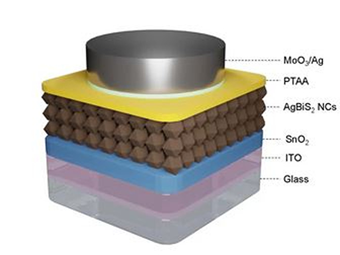
The academics constructed the cell with a substrate made of glass and indium tin oxide (ITO), an electron transport layer (ETL) made of tin oxide (SnO2), the AgBiS2 absorber with embedded NCs, a hole transport layer (HTL) based on poly(triarylamine) (PTAA), a buffer layer made of molybdenum trioxide (MoO3), and a silver (Ag) metal contact.
Tested under standard illumination conditions, the cell achieved a power conversion efficiency of 10.84%, an open-circuit voltage of 0.511 V, a short-circuit current density of 29.15 mA/cm2, and a fill factor of 72.8%. By way of comparison, a control device fabricated without the proposed passivation strategy reached an efficiency of 7.75%, an open-circuit voltage of 0.476 V, a short-circuit current density of 24.98 mA/cm2, and a fill factor of 65.1%.
The researchers said that the efficiency improvement was mainly due to a considerable increase in short-circuit current and fill factor, with the new passivation strategy being responsible for homogenizing cation disorder, which they said improved absorption coefficients and optoelectronic properties. They also found that unencapsulated cells showed a “stable” shelf lifetime under ambient conditions for over 145 days and continuous operation at the maximum power point (MPP) for over 10 hours.
“We believe our work will ignite further interest and attention towards the development of eco-friendly materials and our ink formulation process may find applications in other quantum dot or nanocrystal material systems for photovoltaics or optoelectronics at large,” Konstantatos concluded.
This content is protected by copyright and may not be reused. If you want to cooperate with us and would like to reuse some of our content, please contact: editors@pv-magazine.com.


By submitting this form you agree to pv magazine using your data for the purposes of publishing your comment.
Your personal data will only be disclosed or otherwise transmitted to third parties for the purposes of spam filtering or if this is necessary for technical maintenance of the website. Any other transfer to third parties will not take place unless this is justified on the basis of applicable data protection regulations or if pv magazine is legally obliged to do so.
You may revoke this consent at any time with effect for the future, in which case your personal data will be deleted immediately. Otherwise, your data will be deleted if pv magazine has processed your request or the purpose of data storage is fulfilled.
Further information on data privacy can be found in our Data Protection Policy.