Scientists from Australia and the United Kingdom have developed a novel method for constructing localized rear contacts on p-type silicon absorbers. The proposed process utilizes aluminum (Al) doped and induced polycrystalline silicon (poly-Si) formed at low temperatures.
“This approach avoids the high-temperature processes required for poly-Si formation and the toxic gases involved in in-situ doping through chemical vapor deposition,” they emphasized. “In systems where high-temperature contact fabrication could compromise top cell materials – such as in III-V/Si multijunction solar cells formed through epitaxial growth – this technique offers a valuable alternative.”
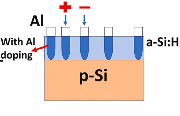
The researchers built the contacts by using p-Si wafers and p-Si substrates, on which they deposited a 45 nm hydrogenated intrinsic amorphous silicon [a-Si:H(i)] layer. They then deposited 400 nm of Al contacts and annealed the samples at 190 C for 5 minutes.
“The surface passivation is damaged due to the presence of Al dopants. Consequently, instead of using a full-area a-Si:H(i)/Al contact, a localized contact structure was chosen to combine the advantages of superior surface passivation of a-Si:H(i) and low contact resistivity introduced by Al-doped poly-Si,” the researchers explained.
Before annealing, the samples exhibited an “insulator-like” behavior. However, once annealed, the sample showed a contact resistivity of 13.17 mΩ⋅cm2. When tested for passivation quality, the area directly beneath Al contacts was significantly degraded post-annealing.
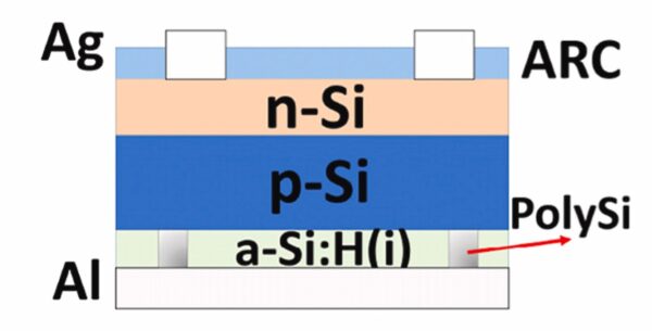
Image: UNSW Sydney, Solar Energy Materials and Solar Cells, CC BY 4.0 DEED
“It should be noted that, however, the a-Si:H(i) layer still provides passivation for areas not covered by Al contacts, despite the reduced passivation quality,” the academics highlighted. “After annealing, the calculated implied open-circuit voltage drop is about 12.7 mV for regions without Al. The preserved passivation and reasonable voltage drop indicate the feasibility of applying this contact technique as localized passivated contacts.”
Following those results, the researchers moved forward to create proof-of-concept solar cells. They were fabricated based on PERC cell precursors of p-Si with a conventional n-type emitter. The front surface was passivated with silicon nitride (SiNx), which also performed as an anti-reflection coating (ARC). Additionally, a 400 nm Al layer was deposited on top to form a full-area Al contact.
For the construction of the rear, the back structure of the PERC cell precursor was removed. A 45 nm a-Si:H(i) layer was then deposited, followed by localized circular Al contacts. The process was then followed by annealing at 190 C for 5 minutes.
“A reference cell based on the PERC precursor featuring a full-area Al back contact was also fabricated for comparison,” the scientists said. “Power conversion efficiencies of 17% and 13.9% were obtained for cells with the a-Si:H(i)/Al contact and a full area Al back contact, respectively, indicating a 3% absolute efficiency enhancement.”
Their findings were presented in the study “Low-temperature aluminum doped and induced polysilicon and its application as partial rear contacts on p-type silicon solar cells,” published in Solar Energy Materials and Solar Cells. The group was formed by researchers from the University of New South Wales (UNSW) Sydney and the University of Oxford.
This content is protected by copyright and may not be reused. If you want to cooperate with us and would like to reuse some of our content, please contact: editors@pv-magazine.com.

By submitting this form you agree to pv magazine using your data for the purposes of publishing your comment.
Your personal data will only be disclosed or otherwise transmitted to third parties for the purposes of spam filtering or if this is necessary for technical maintenance of the website. Any other transfer to third parties will not take place unless this is justified on the basis of applicable data protection regulations or if pv magazine is legally obliged to do so.
You may revoke this consent at any time with effect for the future, in which case your personal data will be deleted immediately. Otherwise, your data will be deleted if pv magazine has processed your request or the purpose of data storage is fulfilled.
Further information on data privacy can be found in our Data Protection Policy.