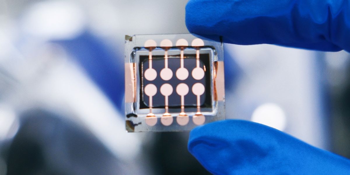
A team led by China's Nanjing University has demonstrated a 0.049 cm2 all-perovskite tandem solar cell with reduced open-circuit voltage losses in the wide-bandgap (WBG) perovskite subcell and improved overall efficiency.
This result was achieved by suppressing non-radiative recombination using a two-dimensional perovskite as an intermediate phase on the film surface. “In our laboratory tests, the device reached a record-breaking efficiency of 29.7%, with an open-circuit voltage of 2.175 V, a current density of 16.4 mA cm-2, and a fill factor of 83.3%,” co-corresponding author Renxing Lin told pv magazine, adding that the result was certified by the Japan Electrical Safety and Environment Technology Laboratory (JET).
The team said that the preferred orientations in wide-bandgap perovskites can be realized by augmenting the quantity of two-dimensional phases through surface composition engineering, without the need for excessive two-dimensional ligands that otherwise impede carrier transport.
The work involved incorporating phenylethylamine iodide (PEAI) and methylammonium iodide (MAI) into the anti-solvent during fabrication, forming a 2D perovskite layer on the surface of the wide-bandgap perovskite subcell.
“This 2D perovskite layer served as heterogeneous nucleation sites, facilitating the vertical growth of (100)-oriented 3D perovskite crystals due to the reduced interfacial energy associated with the 2D/3D heterostructures,” explained Lin. “Consequently, the anti-solvent treatment not only altered the perovskite surface but also significantly influenced the crystallographic orientation of the perovskite crystals, promoting a more advantageous crystal alignment.”
The approach resulted in high-quality WBG perovskite films with a (100) orientation, which suppressed non-radiative recombination in the wide-bandgap perovskite subcells, achieving an open-circuit voltage of 1.373 V for a bandgap of 1.78 eV with 21.1% efficiency.
This was combined with a high-efficiency narrow-bandgap subcell in a tandem configuration, “incorporating a well-optimized optical-electrical matching design” to achieve the high-performance all-perovskite tandem solar cell, according to Lin.
For the WBG films, common approaches were investigated, noted the researchers. One approach added the PEAI into the precursor solution as a direct additive (DA) and the other introduced PEAI into the anti-solvent as a solution-process additive (SPA). Another SPA had a mixture of MAI and PEAI with a weight ratio of 1:2 as the mixed solution-process additive (M-SPA) to create a local MA-rich environment.
Stability tests revealed that both MA specimens “proved more stable” than DA, retaining over 85% of their initial efficiency for 500 hours. However, the one without MA cations performed better. “We suggest that future efforts should focus on non-MA additives that enhance the formation of 2D templates,” said the researchers.
The work is detailed in “All-perovskite tandem solar cells achieving >29% efficiency with improved (100) orientation in wide-bandgap perovskites,” published in nature materials. The researchers were from Nanjing University, ShanghaiTech University, Renshine Solar (Suzhou), and Switzerland’s Ecole Polytechnique Fédérale de Lausanne.
Looking ahead, the group aims to realize the market potential for the technology in utility-scale, residential and other solar PV products. It is also working on efficiency, reliability, and long-term stability, loss reduction and efficiency improvements, including fabrication scaleup from small to large devices.
“To facilitate this, our focus will be on adapting our method for large-area blade coating, a scalable and cost-effective technique for mass production. This will necessitate further optimization of various parameters, including solvent composition, deposition speed, annealing conditions, and coating uniformity, to ensure consistent film quality and high reproducibility across larger substrates,” said Lin. “Additionally, we will address the challenge of maintaining uniformity in the perovskite layers at larger scales, especially regarding the formation of a homogeneous 2D/3D heterostructure at the film surface.”
Further work on interfaces would involve “fine-tuning the materials, layer thicknesses, and encapsulation methods” to enhance device stability. “We are also investigating advanced characterization techniques to gain deeper insights into how the scaling process affects the crystallinity, orientation, and overall morphology of the perovskite films,” said Lin.
This content is protected by copyright and may not be reused. If you want to cooperate with us and would like to reuse some of our content, please contact: editors@pv-magazine.com.


By submitting this form you agree to pv magazine using your data for the purposes of publishing your comment.
Your personal data will only be disclosed or otherwise transmitted to third parties for the purposes of spam filtering or if this is necessary for technical maintenance of the website. Any other transfer to third parties will not take place unless this is justified on the basis of applicable data protection regulations or if pv magazine is legally obliged to do so.
You may revoke this consent at any time with effect for the future, in which case your personal data will be deleted immediately. Otherwise, your data will be deleted if pv magazine has processed your request or the purpose of data storage is fulfilled.
Further information on data privacy can be found in our Data Protection Policy.